Search Results
968 results found with an empty search
- Design Tool Chain for Printed Electronics, Additive PCBs, Smart Surfaces with Printed Sensors, Scaling Up, Highly Conductive MXene
In this issue, we dive into technologies shaping the future of printed electronics and additive electronics, smart buildings, and additive manufacturing. From optimizing tool chains for 3D printed electro-mechanical structures to exploring low-volume manufacturing techniques for printed circuit boards (PCBs), this edition showcases advancements and practical applications. Featured companies include Siemens, Murata Manufacturing, Henkel, and BotFactory, each presenting innovations that are redefining industries. Learn how additive manufacturing and advanced materials are driving efficiency and sustainability in electronics production and smart infrastructure. Siemens | Optimizing the tool chain from Design through manufacturing for Printed Electronics Printed Electronics Ltd | Scaling up From Idea to Product With The PEL Open-Access Printable Electronics Production Facility Henkel - Laiier | Connecting surfaces of the smart building to the cloud with sensors enabled through PE Murata Manufacturing | Highly Conductive MXene for Electronics BotFactory | Exploring AM-PCBs for Low-Volume Manufacturing The Future of Electronics RESHAPED USA is TechBlick's premier event, showcasing the latest innovations in electronics. Join us at UMass Boston on June 11-12, 2025 for an exciting exploration of emerging technologies. You can find more details on the event website here. EARLY BIRD rates are available until December 20, 2025 – secure your spot now! Register here TechBlick.com Siemens | Optimizing the tool chain from Design through manufacturing for Printed Electronics David Wiens | 2023 In this session, you will explore the following: How printing and additive techniques enable innovative electronic architectures, including flexible, conformal, structural, and 3D designs. A comparison of two design approaches: planar structures versus non-planar structures, along with the challenges each presents. The tool chain required for 3D printed electro-mechanical structures, focusing on the key areas of development and optimization. Download the Full Slides Here Printed Electronics Ltd | Scaling up From Idea to Product With The PEL Open-Access Printable Electronics Production Facility Neil Chilton | 2024 For university spin-outs and startup companies, especially in the growing medical sector, it can be challenging to find a responsive production partner to scale up your idea from bench-scale to the small/mid volume production needed to gain investment and customers. PEL is an established manufacturing company with over 18 years’ experience in printable electronics. Here in the UK, we have an extremely well-equipped production facility that gives access to a multitude of printing methods including: high resolution screen printing, inkjet deposition, aerosol jet and viscous jet piezo jet deposition. Whilst some customers prefer to outsource their production entirely to us, we also engage with users who are keen to become manufacturers in the longer term – where they can be trained on the systems we sell and “try before they buy”. In this presentation we explain the capabilities and the training and support packages that PEL can offer. Key takeaways from this session include: Additive manufacturing of electronics – areas of expertise at PEL. Screen printing excellence – featuring high-performance print platforms, including Micro-tec in the EU. PEL's screen print offerings – covering printers, screens, inks, typical layers, and turnaround times. Functional inkjet printing – a detailed example of our inkjet capabilities. Aerosol jetting of bio-compatible carbon electrodes – collaboration with a UK university for disease-sensing applications. Download the Full Slides Here Henkel - Laiier | Connecting surfaces of the smart building to the cloud with sensors enabled through PE Matt Johnson - Laiier | Aad van der Spuij - Henkel | 2022 Step into smart buildings of the future and you might not see a difference. Combining the scalability of coatings and building materials contemporary sensing techniques opens-up an incredible range of possibilities for predictive, preventative, and responsive maintenance. For Henkel, a global leader in specialized and cross-functional ink formulations for printed electronics, and Laiier a smart surface technology provider, the next decade will see the rise of smart buildings that integrate new capabilities into the built environment. Whether it’s office facilities that warn of leaking pipes, walls that heat our rooms, or floors that tell us when an elderly relative has suffered a fall, many of the core technologies are already here. Today, the challenge besides the technology innovation is more about building networks and creating markets. The presentation will cover the unique ecosystem required to bring this vision to life that includes the whole value chain from construction, materials, manufacturing industry to IoT integrators. The session will take the attendees through technical explanations and customer use cases demonstrating clear ROIs and customer insights. In this session, you will learn about: Retrofit Smart Skin: IoT monitoring through smart stickers and tape Unique Selling Propositions: Leveraging printed electronics for installation, coverage, and resolution Surface to Cloud™: Delivering real-time insights and alerts Launch Use Cases: Measuring leaks and levels with "smart tape" Reshaping Partnerships: Accelerating the path to implementation Download the Full Slides Here Join us on February 11-12, 2024, for the Solid-State Battery Materials , a virtual event by TechBlick. Engage with industry leaders driving innovation in battery technology. Explore the agenda here. Early Bird Offer: Register by December 24 and save 150 Euros with the discount code: Save150EurosSSB Register Now https://www.techblick.com/events-agenda Murata Manufacturing | Highly Conductive MXene for Electronics Shun Sakaida | 2022 In this session, explore the potential of MXene (Ti3C2Tx) in electronics applications, with a focus on its high conductivity and environmental stability. Learn about the synthesis procedure for MXene and its ability to enhance components such as capacitors, EMI/ESD components, and SAW components. The session also covers: Schematic Representation: Host–guest interaction for improved environmental stability Humidity Test: Assessing the material's resistance to moisture Anti-Swelling: Strategies to prevent material degradation and maintain performance Download the Full Slides Here BotFactory | Exploring AM-PCBs for Low-Volume Manufacturing Carlos Ospina | 2024 In this session, discover how Additive Manufacturing (AM) is transforming the production of Printed Circuit Boards (PCBs), enabling faster, more sustainable solutions for low-volume manufacturing. Learn about: Reducing Lead Time: How AM reduces the production time of a 4-layer PCB from 10 days to just 4 hours. Challenges of Traditional PCB Manufacturing: The inefficiencies of mass production for small runs. Additive Manufacturing Technologies Matrix: Pros, cons, and how AM fits into low-volume PCB manufacturing. Substrate-Based vs. Substrate-Less: An overview of these different approaches in AM-PCB production. BotFactory’s Experience: Insights into the company's journey with AM-PCBs and the innovations they have implemented. Download the Full Slides Here
- Screen printed heaters, precision digital plasma deposition, 3D AME, Screen printed medical devices
In this edition, we explore exciting breakthroughs shaping the future of electronics. Fernando Zicarelli (E2IP Technologies) dives into the design and challenges of screen-printed heaters, comparing resistive and wire heaters while spotlighting transparent heater advancements. Ram Prasad Gandhiraman (Space Foundry) shares insights into plasma jet printing and its applications in aerospace, tackling issues like adhesion and material performance. Shavi Spinzi (Nano Dimension) showcases the move from 2D to 3D Additively Manufactured Electronics (AME), unlocking new possibilities for compact, high-performing devices. Finally, Marco Galiazzo (Applied Materials) highlights how advanced screen-printing is revolutionizing medical sensor production, offering a cost-effective way to create wearable health-monitoring devices. E2IP Technologies | Screen-printing Heating Devices: Limits and Challenges Space Foundry | Precision digital plasma deposition: deposit multilayer structure without curing Nano Dimension | Roadmap for 3D AME Designs Applied Materials | Advanced Screen-Printing: Manufacture a Medical Sensor by Screen-Printing The Future of Electronics RESHAPED USA is TechBlick's premier event, showcasing the latest innovations in electronics. Join us at UMass Boston on June 11-12, 2025 for an exciting exploration of emerging technologies. You can find more details on the event website here. EARLY BIRD rates are available until December 20, 2025 – secure your spot now! Register here TechBlick.com E2IP Technologies | Screen-printing Heating Devices: Limits and Challenges Fernando Zicarelli | 2024 This presentation will review the most common screen-printed heaters in Printed Electronics; Printed Resistive heaters and Printed Wire heaters. An explanation will follow on how each type of heater is designed, and a comparison between a Printed Resistive heater (PTC) and a Printed Wire heater will be shared. There will be a review of the technology limits and challenges.Finally, a quick review of the latest technological advancements in Transparent heaters. What You’ll Learn in This Session: Why Printed Wire Heaters? Printed wire heaters are incredibly versatile. They can be customized to fit specific shapes and sizes, making them perfect for unique applications. These heaters are often designed with simple yet effective patterns, like serpentines or coils, for even heat distribution. Printed Resistive Heaters vs. Printed Wire Heaters: Explore the differences between these two heating technologies, including how they perform and where they’re best used. What’s Holding Printed Heaters Back? Learn about the key challenges, such as material limitations and design complexities, that researchers and engineers are working to overcome. Download the Full Slides Here Space Foundry | Precision digital plasma deposition: deposit multilayer structure without curing Ram Prasad Gandhiraman | 2023 In This Session, You’ll Explore: Conformal Electronics for Aerospace & Defense: Electromagnetic invisibility for aircraft structures and drones, plus challenges like curing, adhesion, and thickness control. Plasma Jet Printing Technology: How aerosolized ink is used for precise, high-resolution printing. Direct-Write Technology Pain Points: Addressing issues like adhesion, manufacturing complexity, and ink performance. Plasma Deposition & Electrochemistry: Applications of plasma technology in advanced electronics manufacturing. Download the Full Slides Here Nano Dimension | Roadmap for 3D AME Designs Shavi Spinzi | 2022 This presentation will describe the industry drivers for increased electronic devices and circuits performance and packing density and how multi-level and multi-material Additively Manufactured Electronic (AME) technology enables corresponding innovative designs and fabrication from DC to mmWave applications. The presentation will focus on AME devices including design, materials, fabrication, and testing. This technology provides for electronic circuits not only in 2D but also in 3D where connections can be made without vias, but direct wiring between the electronic elements. The wires can be shielded and unshielded. Furthermore, the fabrication technology allows for traces with different thicknesses at the same level. Yielding fully functional boards with smaller size and lower weight, as compared to equivalent PCB fabricated ones. The presentation will include also devices with chip first embedded active ICs. Components such as capacitors, coils, band pass filters, and multilevel Fresnel lenses exhibit superior RF performance as compered Surface Mount Technology (SMT) of components. In This Session, You’ll Explore: AME Fabrication Technology (Nano Dimension implementation) The road from 2D to 3D designs – design examples How to design 3D electronics? Download the Full Slides Here Applied Materials | Advanced Screen-Printing: Manufacture a Medical Sensor by Screen-Printing Marco Galiazzo | 2022 Developments in electronics and sensors have demonstrated the ability to manufacture wearable devices to remotely monitor human health in real-time at reasonable cost. A wide variety of smart sensors are now available, both on rigid and flexibRecentle substrates, to monitor the health and well-being of patients suffering from chronic illnesses. We’ve used our advanced screen-printing capabilities to manufacture medical devices: in particular, we studied and developed the realization of medical sensors entirely by screen printing. Thanks also to the constant improvements of the screen-printing ecosystem (paste, screen, equipment), enabling high processing yields and throughput, manufacturing of such devices by screen printing technology was proven to be a cost-efficient solution, compared to conventional microfabrication techniques, for mass manufacturing of healthcare devices. What This Session Covers: Technical Case Study: Medical Sensors: An in-depth look at remote health monitoring technologies and their applications. An overview of the methodologies and materials used in innovative electronic applications. Silver Traces:Techniques for fine-line printing and the results achieved in precision manufacturing. Carbon Print:Insights into achieving optimal thickness by fine-tuning process parameters. Feasibility Analysis with Applied Tempo™ Presto™ Platforms:Exploring the potential and practicality of using advanced platforms for cutting-edge electronics production. Download the Full Slides Here Join us on December 11, 2024, for the FREE-TO-ATTTEND Printed Electronics & Display Innovation Day , a free online event by TechBlick and the MicroLED Association. Connect with industry leaders shaping the future of displays. View the agenda here. TechBlick.Com
- Exploring Innovations in MicroLEDs and Laser Manufacturing & DeepTech VC Investing
Pyramidal µLEDs, Indium Bump Deposition, InGaN-Based Red Micro-LEDs, Laser and LIFT, VCs In this newsletter, you’ll learn about advancements in microLED technology, deeptech investment, laser-driven manufacturing, and cutting-edge microelectronics. You will also have the opportunity to download the full presentation slides. Polar Light Technologies | Pyramidal µLEDs – a novel - bottom-up concept delivering focused light emission Intlvac Thin Film | Indium Bump Deposition System Kaust | Challenges in InGaN-Based Red Micro-LEDs Technology Coherent | MicroLED Display Volume Manufacturing Enabled By Laser Technology Imec.xpand | Opportunities and Challenges of Investing in Deeptech Startups The MicroLED Connect conference and exhibition will take place next year at the High Tech Campus in Eindhoven on 24 & 25 Sept 2025. You can learn more here This year this show will be co-located with our inaugura l AR/VR Connect t echnology, covering all the key innovations in AR/VR display technology, from light engines to waveguides to optics. EARLY BIRD rates are available until December 20, 2025 – secure your spot now! Register here TechBlick.com Polar Light Technologies | Pyramidal µLEDs – a novel - bottom-up concept delivering focused light emission Lisa Rullik | 2024 Our novel bottom-up concept based on InGaN/GaN uLEDs offers solutions to several challenges that the uLED development is facing right now, namely miniaturization of the die without efficiency droop, sufficient small pitch to reach FHD resolution, and focused light emission to reach sufficient incoupling efficiency into waveguide optics. By using selective area growth, the dies can be placed deterministically onto the lithographically patterned SiN-masked GaN templates and die sizes down to 300nm have been achieved. As no etching of the die itself is needed the efficiency of the InGaN quantum wells, which are the active emitters, stay intact. The geometic structure of the uLED, a hexagonal pyramid, facilitates the focused emission and a sub-lambertian emission was obtained. In this presentation you will learn about the following: Polar Light Technologies’ GaN/InGaN bottom-up approach without etching damage Achieving RGB in the same material system Focused light emission and sub-lambertian performance Insights from the first hybridization prototypes Download the Full Slides Here Intlvac Thin Film | Indium Bump Deposition System Michael Chesaux | 2024 Producing indium bumps for interconnect is a technology that has had to adapt to an ever increasing demand for smaller bump size and high bump density while having to process larger and larger substrate sizes. This presentation discusses how indium bump fill and uniformity was optimized for substrates up to 200mm wafers. We demonstrate strategies to both prevent dendritic growth, to produce reliable bumps, and to eliminate indium spits, which can be a source of defects, without having to sacrifice tack time and reliability. In this presentation you will learn about the following: How we minimized pattern hole closure How we improved bump quality by preventing dendritic growth Prevention of spits System stability and reliability Indium bumps we produce Download the Full Slides Here Kaust | Challenges in InGaN-Based Red Micro-LEDs Technology Daisuke Iida | 2024 Micro-LEDs are promising for next-generation displays such as AR/VR. InGaN material can generate emissions in red, green, and blue. In the same material system, the LED devices can be stacked continuously, making it possible to fabricate monolithic RGB micro-LEDs on the same wafer. The low efficiency of red LEDs is the bottleneck for RGB micro-LED development. In this presentation, we will discuss the growth technology for InGaN-based red LEDs and the realization of monolithic RGB micro-LEDs. In this presentation you will learn about the following: Red LED growth technologies Micro-LED fabrication technologies Monolithic RGB micro-LEDs LED Fabrication Technologies Download the Full Presentation Slides Here Join us on December 11, 2024, for the FREE-TO-ATTTEND Printed Electronics & Display Innovation Day , a free online event by TechBlick and the MicroLED Association. Connect with industry leaders shaping the future of displays. View the agenda here. TechBlick.Com Coherent | MicroLED Display Volume Manufacturing Enabled By Laser Technology Oliver Haupt | 2024 Laser technologies are essential for display fabrication today. Several laser processes and laser types are required for state-of-the-art display manufacturing. With the move from OLED to microLED displays some processes remain and several new manufacturing processes are required. The success of microLED displays is mainly driven by costs and availability of volume manufacturing equipment. Thus, microLEDs must become very small and need to be processed with highest throughput and yield. Lasers have proven their capability already in many applications but also in display fabrication. In this presentation, we will provide an overview of the microLED display process chain and highlight the individual laser processes. In this presentation, you’ll learn about Laser-driven mass transfer techniques like LIFT The key steps in microLED manufacturing and how lasers drive innovation. The critical role of laser mass transfer for microLED miniaturization. Advanced laser applications like LTPS backplane annealing and beam delivery systems. Download the Full Presentation Slides Here Imec.xpand | Opportunities and Challenges of Investing in Deeptech Startups Cryil Vancura | 2024 Many aspects of today’s modern society are enabled by advances in semiconductor technologies. Most of those innovations have been driven by the incumbent corporates in the industry but some of them have come from ambitious startups globally. Despite the size of the market and the potential for key innovation, startups active in semiconductor technologies have often struggled to raise sufficient capital in the past decade, even in times when other sectors of the venture capital market have been very active. Since one to two years, though, we start to see a change in sentiment of venture capital investors towards semiconductor technology startups. This is driven by external market factors, such as the onset of artificial intelligence technology, driving global increase of data center traffic and compute performance, as well as geopolitical considerations and dependencies.imec.xpand is one of the world’s largest independent venture capital funds dedicated to early-stage semiconductor innovation. Since 2018 we have been investing in ambitious startups where the knowledge, expertise and infrastructure of imec, the world-renowned semiconductor and nanotechnology R&D center, can play a determining role in their growth. imec.xpand has an outspoken international mindset towards building disruptive global companies and strongly believes that sufficient funding from the start is key to future success. Our position gives us a unique view on the startup landscape in the sector, which we will share with the audience. In this presentation, you’ll learn: How imec's world-class infrastructure, brilliant minds, and global network enable disruptive ventures. What venture capitalists look for, including team evaluation and market potential. The importance of understanding the value chain, business models, and positioning in the market. Strategies for building a competitive edge, from patents to speed and comprehensive approaches combining these elements. Download the Full Presentation Slides Here Join us on December 11, 2024, for the FREE-TO-ATTTEND Printed Electronics & Display Innovation Day , a free online event by TechBlick and the MicroLED Association. Connect with industry leaders shaping the future of displays. View the agenda here. TechBlick.Com
- Photovoltaics: R2R Processing, CZTS Printing, Large Scale Perovskite, Laser Assisted Glass Encapsulation, Perovskite Stability, etc
In this newsletter, explore the advancements in solar technology, featuring InterPhases Solar's pioneering in-line roll-to-roll processes for flexible, thin-film devices, Crystalsol OÜ's innovations in CZTS photovoltaic technology, Taiwan Perovskite Solar's approach to large-scale perovskite production, Pixel Voltaic's laser-assisted glass encapsulation for perovskite photovoltaics, and University of Colorado Boulder's strategies to tackle degradation in perovskite solar panels. InterPhases Solar | Versatile in-line roll-to-roll process for flexible, thin film devices Crystalsol OÜ | Printed CZTS photovoltaic technology Taiwan Perovskite Solar | Large-scale perovskite production: materials, processes, and challenges Pixel Voltaic | Laser-assisted glass encapsulation for perovskite photovoltaics University of Colorado Boulder | Understanding & preventing degradation in perovskite solar panels The Future of Electronics RESHAPED USA is TechBlick's premier event, showcasing the latest innovations in electronics. Join us at UMass Boston on June 11-12, 2025 for an exciting exploration of emerging technologies. You can find more details on the event website here. EARLY BIRD rates are available until December 20, 2025 – secure your spot now! Register here TechBlick.com InterPhases Solar | Versatile in-line roll-to-roll process for flexible, thin film devices Shalini Menezes | 2024 Fabricating devices with non-vacuum roll-to-roll processes that intrinsically host nano-scale pn junctions offer an attractive platform to create low-cost, flexible, lightweight opto-electronic devices. Incumbent 3G nano technologies still face significant challenges in-terms of stability, toxicity, up-scaling and reproducibility to reach the status of the established technology. Here we present an alternate path that integrates new device structure, process and manufacturing. It features a compact, practical, atmospheric process to manufacture high quality, ordered 3D nanocrystalline pn homojunction (NHJ) device structures. Exemplified here by two Cu-In-Se (CISe) compounds, the method entails single-step electrodeposition of interconnected network of p-CISe and n-CISe nanocrystals to create a depleted NHJ thin film. Extraordinary attributes the CISe NHJs include non-linear emissions, large carrier mobility, low trap-state-density, long carrier lifetime and likely up-conversion. The NHJ film can be inserted between two electrodes to produce an isotropic device, wherein current can flow in either direction to convert light into electricity or applied voltage into light. Although originally conceived for CISe solar cells, this radical concept could create NHJs with most II-VI or III-V semiconductors for wide spectrum of applications, e.g., PV panels, LEDs, photodetectors, photoelectrodes, laser diodes, displays, MEMS and optical fibers. Importantly, the NHJ structure can be continuously roll-to-roll processed in ambient atmosphere from aqueous solution. Overall, this approach offers a promising low-cost processing platform to create high performance, stable and scalable devices. The NHJs could essentially perform like 2D planar pn junctions or artificially ordered 3D nano-structures, but without their high cost and fabrication complexities. In this presentation you will learn about the following: 2D & 3D Opto-Electronic Devices: Exploring the challenges of achieving 2D performance in 3D manufacturing processes. CISe: Cu-In-Se approach demonstrated SSE: Single-step electrodeposition NHJ: Nanocrystalline pn homojunctions with unusual nano & quantum attributes R2R: Roll-to-roll manufacturing Download the Full Slides Here Crystalsol OÜ | Printed CZTS photovoltaic technology Dieter Meissner | 2024 In this session, you will explore the following topics: Why printing, but not OPV (Organic Photovoltaics) CZTS/Kesterite: Powder production, powder composition, and stability of Kesterites with different chalcogenide ratios Powder (monograin) printing technology, powder synthesis (high T.), and module printing (low T.) in a continuous roll-to-roll process Crystalsol monograin cell and module printing Efficiency and stability potential Cost considerations Sustainability Download the Full Slides Here Taiwan Perovskite Solar | Large-scale perovskite production: materials, processes, and challenges Chih-Hsuan Chao | 2024 In the field of solar energy, it has become a common belief that perovskite solar cells are advancing at an unprecedented pace. While the historical trajectory may seem astonishing, we can gain insight by examining the development path of the solar cell industry, which has progressed from silicon and CIGS (copper indium gallium selenide) to organic solar cells. Perovskite solar cells represent the culmination of decades of knowledge and research. A perovskite solar cell is composed of multiple layers. Each layer is carefully deposited on a substrate, which imposes certain limitations on the choice of materials and manufacturing processes for the top layer. To overcome these limitations, various process technologies such as slot-die coating, blade-coating, and spray deposition have been developed and refined for large-scale production. Additionally, a wide range of materials has been extensively studied. In the presentation, we will delve into the critical considerations for selecting materials and processes when fabricating perovskite solar cells. Furthermore, we will highlight the challenges and obstacles associated with these technologies. This session will cover the following topics: Structure of PSC: Conventional & Inverted Material selection and process considerations Techniques for creating thin film layers Classification of coating methods and choosing the right solution Encapsulation processes Download the Full Slides Here Join us on December 11, 2024, for the FREE-TO-ATTTEND Printed Electronics & Display Innovation Day , a free online event by TechBlick and the MicroLED Association. Connect with industry leaders shaping the future of displays. View the agenda here. TechBlick.Com Pixel Voltaic | Laser-assisted glass encapsulation for perovskite photovoltaics Tiago Lagarteira | 2024 This session will delve into: Power Conversion Efficiency (PCE) of 3rd Generation PVs The necessity of glass encapsulation for PSCs Glass frit encapsulation process for PSCs Innovative solutions in glass frit encapsulation Download the Full Slides Here University of Colorado Boulder | Understanding & preventing degradation in perovskite solar panels Mike McGehee | 2024 Metal halide perovskites are ionic conductors and can undergo oxidation and reduction. Perovskite solar cells often contain metal electrodes that can be oxidized. Redox reactions occur quite rapidly when the cells are operated in reverse bias, which can happen when a shaded cell is forced to match the current of illuminated cells that are connected in series. Shunting typically occurs in reverse bias when silver electrodes are used, but not when transparent conducting oxides or carbon are used. Oxidation of iodide can result in loss of iodine from the perovskite layer, which can also reduce power conversion efficiency. The talk will describe the electrochemical degradation and how feasible it is to protect different types of modules with bypass diodes. This session will explore: The future of module manufacturing with perovskite solar cells, including the potential dominance of classic thin-film processes unless perovskite-Si tandems are adopted. The challenges of laser scribing, such as stability issues and thermal damage during the ablation process. Why perovskite-Si monolithic tandems eliminate the need to cut through the ITO electrode. How current can pass in reverse bias, either through uniform tunneling or metal shunts. The lack of demonstrated perovskite cells that remain stable under reverse bias for extended durations. Download the Full Slides Here Join us on February 11-12, 2024, for the Solid-State Battery Materials , a virtual event by TechBlick. Engage with industry leaders driving innovation in battery technology. Explore the agenda here. Register Now TechBlick.Com
- Advancements in Additive Electronics Manufacturing and Printing Technologies
In this newsletter, you’ll explore cutting-edge innovations in additive electronics manufacturing, bioprinting, and printed electronics. Gain insights from industry leaders and download the full presentation slides to dive deeper into these transformative technologies. ImageXpert | Inkjet & Dispensing for Printed Electronics: R&D to prototype and Pilot Production University of Montreal | Drop-on-demand laser-assisted bioprinting of cells & hydrogels Fraunhofer IAP | Inkjet printable stretchable electrodes for organic electronic applications NRCC | Material & Process development for additive manufacturing TNO at Holst | 3D Additive Lithography for Electronics The Future of Electronics RESHAPED Boston is the flagship TechBlick event. This event will take place at the UMass Boston, USA on the 11-12 June 2025. Visit the event website here. EARLY BIRD rates are available until December 20, 2025 – secure your spot now! Register here TechBlick.com ImageXpert | Inkjet & Dispensing for Printed Electronics: R&D to prototype and Pilot Production Paul Best | 2023 In this presentation, ImageXpert will discuss new technologies in inkjet for evaluating and optimizing processes in R&D and production. These tools allow you to build a better understanding of your inkjet process, improve the performance, and accelerate the rate of development. We will explore the latest analysis tools, from new dropwatching technologies to smarter prototyping printers. In this presentation you will learn about the following: A Process for Optimization in Jetting/Dispensing Performance: Volume, Velocity, Trajectory, Satellite, Wetting, Print Quality Measurement: Feature Size, Dot Positioning, Edge Quality, Uniformity, Drop Impact Testing Inkjet Performance, Sustainability – Drop Analysis. Measuring Nozzles Across the Head, Testing Inkjet Performance JetXpert Print Station Optimizing Inkjet Performance:Pulse Width, Damping Pulse Spacing, Voltage Download the Full Slides Here University of Montreal | Drop-on-demand laser-assisted bioprinting of cells & hydrogels Christos Boutopoulos | 2023 Learn about: Cell bioprinting technologies: Viscosity range, resolution, speed, and cell viability Laser-Induced Side Transfer (LIST) for precise bioprinting Liquid ejection dynamics in LIST: Optimal printing conditions and maximum speed Microvasculature bioprinting and the role of pro-angiogenic factors in tubulogenesis Download the Full Slides Here Fraunhofer IAP | Inkjet printable stretchable electrodes for organic electronic applications Manuel Gensler | 2023 In this presentation you will learn about the following: The fundamentals of stretchability in PEDOT:PSS materials Ink development for heart-rate sensor applications in collaboration with Umana Medical Dielectric Elastomer Actuator with inkjet printed electrodes Download the Full Slides Here Join us on December 11, 2024, for the FREE-TO-ATTTEND Printed Electronics & Display Innovation Day , a free online event by TechBlick and the MicroLED Association. Connect with industry leaders shaping the future of displays. View the agenda here. TechBlick.Com NRCC | Material & Process development for additive manufacturing Chantal Paquet | 2023 In this presentation you will learn about the following: Molecular inks (M-INKs) -Metal salts (e.g. copper formate, silver carboxyates) formulated into inks that decompose to form a metal film 2D printing: Boron nitride nanotube (BNNTs) coatings on PET to improve performance of printed conductors 2.5D printing: In-mold electronics with molecular inks 3D printing: Silver neodecanoate in photoresins for 3D printing of conducting structures Download the Full Slides Here TNO at Holst | 3D Additive Lithography for Electronics Jeroen Sol | 2023 In this presentation you will gain insights on the following: Lead Extractor Use Case: Enabling localized ultrasound imaging for safer heart pacemaker lead replacement procedures. Innovative Design: A 6 mm diameter ring-shaped device with 10 chips, integrated seamlessly using 3D-ALE, eliminating the challenges of traditional assembly. 4D Printing Benefits: Accelerated design iterations and faster time-to-market through this cutting-edge technique. Download the Full Slides Here Join us on December 11, 2024, for the FREE-TO-ATTTEND Printed Electronics & Display Innovation Day , a free online event by TechBlick and the MicroLED Association. Connect with industry leaders shaping the future of displays. View the agenda here. TechBlick.Com
- Voltera | Printing a Magnesium Zinc Battery with Saral Inks on PET
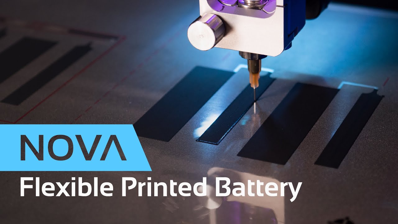
Author: Jesus Zozaya , CEO at Voltera | sales@voltera.io As presented at the TechBlick Berlin event in October, our project, a multilayer magnesium zinc battery, validated the compatibility of Saralon’s battery inks printed on a PET substrate. Watch our Video: Printing a Flexible Magnesium Zinc Battery with Voltera NOVA MATERIALS USED Saral Silver 600A Battery Ink Saral Carbon 700A Carbon Based Conductive Ink Saral Zinc 700 Battery Ink Saral MnO2 800 Battery Ink Saral BatBarrier 600 Battery Ink Saral HotMeltGlue 800 Battery Ink Saral BatElectrolyte 700 Battery Ink SUBSTRATES USED Polyethylene terephthalate (PET) TOOLS AND ACCESSORIES Voltera NOVA materials dispensing system Nordson EFD 7018302 dispensing tip (330 µm ID) Nordson EFD 7018107 dispensing tip (840 µm ID) Nordson EFD 7018260 dispensing tip (410 µm ID) Nordson EFD 7018333 dispensing tip (250 µm ID) Heat press machine Dual asymmetric centrifugal mixer Project Overview Purpose The purpose of this project is to demonstrate how we fabricated a functional multilayer printed battery on a flexible PET substrate, validating the compatibility of PET with a variety of conductive and insulating inks. Image: Printed flexible battery-powering lights in a breadboard Design layout Typically, a printed battery consists of five layers: Current collector layer for the anode Anode layer Separator layer with electrolyte Current collector layer for the cathode Cathode layer Image: Schematic for typical printed batteries We segmented the battery into halves, each comprising four units, connected in series. As a result, our final print consisted of seven layers. Image: Design layout The printing sequence was as follows: Silver conductive layer Carbon current collector layer Zinc anode layer Manganese dioxide cathode layer Separator layer Hot melt glue layer Zinc chloride electrolyte layer Desired outcome Once the halves are laminated together, the cells align perfectly and do not exhibit any leakage. When connecting its two probes to the battery terminals, the multimeter shows a stable reading of about 2.4 V. Functionality The device incorporating the Saral inks was able to operate at a voltage of 2.4 V, which can make the battery quite versatile. With a voltage of 2.4 V, a printed battery can power a range of devices from low-power electronics such as LEDs, to more demanding applications such as handheld GPS devices, depending on its capacity. The dimensions for the battery are 90 mm L × 85 mm W × 0.75 mm H, with an initial capacity of about 1 mAh. Larger energy capacity and different voltages are achievable by varying the size and thickness of the layers, choosing different materials for electrochemical reactions, or adding more cells in series. We are speaking at the Free-To-Attend Online Printed Electronics Innovation Day Printing the magnesium zinc battery Silver conductive layer This layer consists of a silver conductive circuit connecting the positive and negative terminals. The Saral Silver 600A Battery Ink used for this layer provides a moderate electrical conductivity (< 20 mΩ/sq at 25 μm), ensuring reliable current flow between the electrodes. NOVA settings, silver conductive layer Image: Silver conductive layer design Image: Silver conductive layer print result Carbon current collector layer This layer consists of carbon features that collect current from both the anode and cathode, covering all eight cells (the basic units that generate electrical energy through electrochemical reactions) across the halves. The Saral Carbon 700A Carbon Based Conductive Ink provides excellent adhesion on PET, with a moderate resistance of 30 Ω/sq at 25 μm, ensuring efficient collection of current. NOVA settings, carbon current collector layer Image: Carbon current collector layer design Zinc anode layer This layer includes four cells that serve as the anode of the battery. The Saral Zinc 700 Battery Ink provides a sufficiently thick layer by one print, ensuring that the anode maintains a high conductivity and stability throughout its lifecycle. The high zinc content promotes efficient electron flow, which is critical for maintaining the battery's overall energy output and longevity. NOVA settings, zinc anode layer Image: Zinc anode layer design Image: Zinc anode layer print result Manganese dioxide cathode layer This layer includes four units that serve as the cathode of the battery. Similar to the The Saral Zinc 700 Battery Ink, the Saral MnO2 800 Battery Ink provides a sufficiently thick layer by one print, ensuring that the cathode maintains a high conductivity and stability throughout its lifecycle. NOVA settings, manganese dioxide cathode layer Image: Manganese dioxide cathode layer design Image: Manganese dioxide cathode layer print result Separator layer This layer consists of eight units printed with a water-based ink to create separation between the anode and the cathode layers. Once dried, it becomes porous to allow ion travel. NOVA settings, separator layer Image: Separator layer design Image: Separator layer print result Hot melt glue layer Excluding the terminals, anodes, and cathodes, this layer covers the whole surface of the final print and facilitates lamination. NOVA settings, hot melt glue layer Image: Hot melt glue layer design Image: Hot melt glue layer print result Zinc chloride electrolyte layer This layer consists of eight units of electrolytes, each slightly smaller than the anode/cathode units. They provide electrolytes that facilitate the movement of ions between the anode and cathode. NOVA settings, zinc chloride electrolyte layer Image: Zinc chloride electrolyte layer design Image: Zinc chloride electrolyte layer print result Laminating the halves of the printed battery together Once the last layer was printed and dried, we cut out part of the PET substrate to leave the terminals exposed. We then folded the print from the middle, carefully aligning the fiducial marks. Next, we inserted the PET into the laminator at 120°C, with the terminals going in last. This was to prevent leakage of the electrolyte to neighboring units and causing short circuits in the battery. When subjected to heat, the hot melt glue layer becomes sticky and holds the halves together. Image: Printed flexible battery folded and laminated Challenges and advice for printing batteries on flexible substrates Nozzle compatibility Nozzle clogging was an issue while working on the separator layer, which was printed with an ink that tends to dry quickly and is prone to forming agglomerates if left unused for an extended period. In addition, due to the thin, water-like consistency of the water-based BatBarrier 600 Battery Ink, we had to refine print settings to adjust for over-dispensing in order to achieve the intended thin, uniform traces. We mixed the ink using a dual asymmetric centrifugal mixer before printing. This process, which lasted for 10 minutes at a speed of 2,000–2,500 rpm, proved effective in breaking up the agglomerates and alleviating clogging. Additionally, removing excess water from the ink (we removed 1.8 mL) helped resolve issues with over-dispensing. Layer leakage Because the electrolyte layer was printed with a water-based zinc chloride ink, it posed some challenges during lamination. To avoid leakage, we noted that sufficient time was required for the electrolyte layer to absorb into the separator layer before laminating the halves together. As the design varies, the volume of inks dispensed is different. It is therefore difficult to pinpoint an exact time required for the electrolyte layer to absorb. Some visual signs that indicate full absorption include: ● A noticeable lowering of the level of the electrolyte layer ● Drying and uniformity of the print surface ● A change in the color of the electrolyte layer to a dull white hue It is also important to note that achieving a higher short circuit current usually involves increasing the thickness and size of the electrolyte layer. Consequently, more time should be allowed for the layer to dry and settle properly. Conclusion The thickness of the final print (excluding the PET substrate) is 500 µm, which highlights the potential of printed batteries to be ultra thin and flexible. More importantly, this flexibility renders printed batteries highly customizable — they can store energy in various shapes and sizes to suit product design, instead of the other way around. In this project, we experimented with zinc and magnesium dioxide inks as the anode and cathode, but a wide variety of materials can be used for printed batteries, including lithium cobalt oxide, carbon nanotubes, and vanadium oxide, to name a few. As we continue to explore the possibilities of printed batteries, we invite you to view the other application projects we’ve completed. As we continue to explore the possibilities of printed batteries, we invite you to view the other projects we’ve completed. If you’d like to discuss your designs or our NOVA materials dispensing system, please book a meeting with our applications team or contact us at sales@voltera.io . We are exhibiting! Visit our booth at two flagship TechBlick's events (1) in Boston on 11-12 June 2025 and (2) in Berlin on 22-23 October 2025 . Let's RESHAPE the Future of Electronics together, making it Additive, Sustainable, Flexible, Hybrid, Wearable, Structural, and 3D.
- Copper microparticle conductive ink for low-cost RFID antenna printing | Saralon GmbH
Author: Steve Paschky ( steve.paschky@saralon.com ) I recently read an insightful article on Nature about the challenges facing the scale-up of the Printed Electronics industry [1]. The article effectively highlights how disruptive technologies, like those in our industry, are reshaping the electronics landscape. While we often associate this sector with innovation, not every innovation is truly disruptive. Disruptive innovations fundamentally change industries, even society and lifestyle. PE innovations don’t just add value; they also revolutionize how electronics are produced, replacing traditional methods. As a materials supplier for PE industry, Saralon GmbH has started with engaging into emerging markets that didn’t exist before. Some of our best-selling Saral Inks© with high demands from these markets include SaralBattery Inks and Stretchable Saral Inks © among many others. However, as disruptive innovations evolve and mature, the key challenge becomes aligning them with mainstream markets. This is where the concept of product-market fit becomes critical. Saral Copper 200 is our latest generation of copper conductive ink designed with product-market fit in mind. While it has the potential to be used in conventional PCB manufacturing (thanks to its solderability), the primary market we are focusing on is smart labelling, smart packaging, and antenna technology at the core—specifically RFID and NFC tags and inlays. Before diving into the details of Saral Copper 200, I’d like to briefly elaborate on why copper ink and how it addresses the gaps in current solutions in the mainstream antenna market. 1. Huge market potential The smart labeling market is rapidly growing. In 2023, the global market for NFC and UHF tags was valued at 7 billion euros, and it’s projected to grow at a compound annual growth rate of 15%. Despite this growth, most RFID antennas are still made through unsustainable, subtractive etching process. IDTechEx says that only around 1.5% of antennas are produced by additive manufacturing processes. This highlights a significant opportunity for innovation in the Printed Electronics industry. 2. Additive printing vs. conventional subtractive electronics manufacturing Etching, the dominant antenna production method, is unsustainable. It wastes materials and relies on corrosive chemicals. Additionally, this process can only produce high-volume standardized antennas. Printed Electronics offer a sustainable, additive manufacturing alternative that allow for the production of customized antenna tags and inlays. However, current printed electronics solutions rely on silver conductive inks, that brings up the challenge of cost. 3. Copper microparticle conductive ink to deal with the cost issue While antennas including RFID inlays, NFC tags, etc. play a central role in smart labelling and retailing applications, cost has remained to be the key challenge for vast commercialization of Printed Electronics antennas. Up until today, printed antennas have primarily used costly silver-based materials making them less viable for large-scale adoption. Due to the rising and volatile silver prices, Printed Electronics community recognizes the pressing need to develop conductive inks made of lower cost underlying materials. In addition to being more affordable, such an alternative must provide comparable conductivity while ensuring ambient stability over time, and easy processability using conventional printing technologies (i.e. screen printing). Saral Copper 200 is a thermal curable copper microparticle based electrically conducting ink, suitable for paper and different plastic substrates. The ink is simply screen printable and thermally curable. Processed due to the instructions, a sheet resistance of 17 mΩ /sq/25 μm is easily accessible for printed and dried Saral Copper 200 with excellent ambient stability over time. In short, main advantages of Saral Copper 200 include: Dramatically lower cost Simply screen printable and hot air curable Low sheet resistance and excellent ambient stability Significantly lower carbon footprint compared to silver Saral Copper 200 is the revolutionary solution for the Printed Electronics industry to overcome cost challenges, particularly in the high-volume markets of smart labelling and RFID antennas which are currently dominated by conventional electronics that depend on unsustainable etching methods. Saral Copper 200 allows for the additive manufacturing of smart labels directly near the end-use markets. This will significantly reduce both costs and emissions associated with long-distance transportation. The demand for RFID tags and smart labeling is strong, the enthusiasm is present, and the opportunity is within reach. We’ve developed Saral Copper 200 with a product-market fit mindset to empower Printed Electronics industry in terms of cost effectiveness, performance, sustainability, and easy processability. I am Speaking Printed Electronics Innovation Day - 11 December 2024 This is a free-to-attend online conference and exhibition organized by TechBlick. It is co-located with TechBlick Display Innovation Day (online). We invite you to attend and listen to our talk. [1] https://doi.org/10.1038/s44287-024-00096-9
- Intellivation LLC Welcomes Dr. Robert Malay as New Application Lab Director
by Austin Buchholtz | Nov 12, 2024 INTELLIVATION LLC is thrilled to announce the addition of Dr. Robert Malay to our team as the new Application Lab Director. The Application Lab includes two R2R Vacuum Coating systems and our Laser system for patterning and annealing thin film coatings. Dr. Malay brings extensive expertise in deposition on flexible substrates, physical vapor deposition (PVD), characterization, and experience with application and industrial integration for end users. This strategic addition will bolster our technology development and customer support efforts. In his new role, Dr. Malay will oversee all Application Lab activities including deposition of single and multilayer coatings on flexible substrates, materials characterization, and precision patterning and annealing of deposited films. He will also assist the product development department with testing of new systems for commercial use. His broad experience will be instrumental in enhancing existing and new products to assure that Intellivation continues to provide industry-leading hardware and software in our systems. "We are excited to welcome Dr. Robert Malay to Intellivation LLC," said Mike Simmons, President & CEO. "His vast experience and dedication to advancing technology make him a perfect fit for our team. We look forward to the innovative solutions and support he will bring to our customers and growing capabilities in our Application Lab.” Dr. Malay will also play an important role in representing Intellivation at industry-leading organizations such as Association of Roll-to-Roll Converters (ARC), the Society of Vacuum Coaters (SVC) and International Converting Exhibition (ICE), furthering our commitment to supporting our industrial partners and staying at the forefront of technological advancements. Dr. Malay received his PhD from Binghamton University, where his research focused on R2R electronic device fabrication, projection lithography and characterization on flexible glass. Please join us in welcoming Dr. Rob Malay to Intellivation LLC. We are confident that his contributions will drive our ongoing success and innovation. Contact Information: Intellivation LLC 560 W 66th Street Loveland CO 80538 info@intellivation.com www.intellivation.com Follow us on LinkedIn
- Intellivation LLC Press Release: 2024 Technology of the Year Award Winner
October 30, 2024 - Intellivation LLC is honored to have been awarded the Technology of the Year Award from the Association of Roll-To-Roll Convertors (ARC) for our unique and innovative solution to measure Mid-IR Reflectance In-Situ with Spectrometry in our R2R Vacuum Sputter Coaters. “We are excited to introduce the first production solution using spectrometry to measure in-situ in this spectral range in a vacuum R2R coating system. As requirements and applications use broader spectral ranges and become more sophisticated, we see increase demand for monitoring sputtered multi-layers in-situ,” says Mike Simmons, President & CEO of Intellivation. “Our customers are redefining the standards for end use requirements and we are extremely proud to be a part of the solution. Receiving this Award from ARC, which represents the entire industry of Roll-to-Roll converting and manufacturing processes, is an incredible honor, and we are so appreciative.” The ability to expand the spectral range to reach the Mid-Infrared (Mid IR) spectrum can create new opportunities and applications for sputtered thin film use. The integration of a Mid IR Tunable Quantum Cascade Laser (QCL) based reflectance spectrometer into a Roll-to-Roll (R2R) Sputter Coater offers enhanced spectral resolution and tunability, allowing for precise and selective analysis of Infrared optical materials during the coating process. Integrating this advanced spectrometer into a R2R Sputter Vacuum Coater enables real-time monitoring and control of thin film deposition, facilitating improved process optimization. The ability to monitor reflection beyond the current UV and visible ranges, into the Mid IR wavelength (8 to 13 microns) contributes to the development of a much wider range of functional layer materials and provides a versatile and efficient manufacturing platform for high-throughput production of coated materials with tailored optical properties, offering new possibilities for applications in various industries. Coatings and multi-layers in the Mid IR range can provide optical functions that enable environmental protection for devices and systems from light, humidity, and stress that can be induced by the environment and outside influences. These coatings can extend the life and/or improve durability of components in a wide range of applications and industries, many of which are just being developed. In-situ Mid IR reflection monitoring of vacuum roll-to-roll coatings improves development and production yield of highly complex and multi-functional layer stacks used in high tech industries and applications. Intellivation is a leading manufacturer of vacuum web coating equipment featuring unique and innovative state-of-the-art design with powerful automation. We offer R2R Series vacuum coaters and metallizers in widths from 330mm to 2m which can include rotary and planar magnetrons, evaporation technology, substrate pretreatment, and in-situ monitoring. Our on-site Application Lab featuring R2R330 and R2R600 roll-to-roll vacuum coaters provides the ability to support customers’ thin film coating development on flexible substrates including metal foils, polymers, textiles, nonwovens, flexible glass and flexible ceramics. We provide solutions for technically challenging applications including but not limited to medical devices, energy storage, superconductors, optics, flexible electronics, solar and other functional coatings. We continue to grow and currently are hiring for multiple positions. Please contact jobs@intellivation.com for information or visit our Indeed posts. Job Postings - INTELLIVATION | Engineered Solutions For more information: info@intellivation.com or www.intellivation.com
- Discover The Secretes Of Printed Heater Design Now - A Design Guidebook
Author: Dr. H David Rosenfeld, h.rosenfeld@celanese.com Electrical resistance heaters Electrical resistance heaters can take many forms. They might be wires, ceramics, textiles, films, printed conductive inks and pastes, or some other form. Regardless of form, they all work on the principle of Joule Heating, where a flow of current through a resistance creates heat. The rate of heat production (power) is proportional to the square to the current. The coefficient of proportionality is the resistance of the conductive element, Ohm's law, V=IR, relates current to voltage allowing this to be written This last form is most useful, since voltage is typically specified, and the resistance is selected to fix both the current and the power to desired levels. All electrical resistance heaters are 100% efficient in converting electrical energy into heat. Electrical power in equals heating power out. However, the physical form of the heating element can have a big impact on how that heat flows away from the heating element towards the surface that is to be heated. Film heaters, made by printing functional inks/pastes onto a flexible substrate can be very effective in delivering heat to the surface of a seat, a panel, or the wearer of a heated garment. Unlike metal wire heaters, the power is produced over a large area. The thermal gradient it produces is effectively unidirectional and heat flows directly toward the desired surface. Printed film heaters are thin and smooth. They don’t need to be padded to prevent them from printing through or causing user discomfort. This means faster warm-up and less energy wasted heating the thermal mass of the padding. For these reasons, printed film heaters can deliver the same thermal performance on the surface of interest with less energy input. In this way, they can be said to be more efficient in converting input power to surface heating. Printed PCB carbon film heater Functional pastes for printing film heaters can be either fixed resistance or so-called positive temperature coefficient (PTC) pastes. The later having the property of increasing resistance with increasing temperature. Since heating power is proportional to resistance, this means they produce less power as they get hot. They are sometimes referred to as self-regulating. Micromax™ has several PTC pastes to select from with different resistance responses to temperature. An example is PTC085, which rapidly increases resistance as its temperature approaches 85C. More on this later. Fixed resistance pastes can be used to print two styles of heater circuit. A highly conductive paste can be printed in a serpentine pattern to mimic the design of a wire heater. We call this style a printed wire. Printed wire heaters are usually made with silver conductive pastes. The high conductivity is needed to allow for a long trace with sufficiently low resistance. An example is shown in figure 1. Figure 1. Photo of printed wire heater (butterfly heater). Silver with carbon overprint. Both PTC and non-PTC pastes can be used to form tile heaters. These are created by running two parallel busses of a high-conductivity paste with inter-digitated fingers extending between them. One bus is positive, and the other is negative. Tiles of a less conductive paste are then applied to connect opposing fingers (Fig. 2). The tiles are the heating elements and are usually formed with a carbon-based paste, either fixed resistance or PTC. It is best if the tiles are kept small, on the order of a centimetre or less in any dimension, in order to avoid hotspots caused by the uneven thickness of the print. This usually requires the paste to have a high sheet resistance as printed. A few hundred Ω/□ (ohms/square) or more. PTC carbon pastes fit this requirement very well. Figure 2. Tile heater (seat heater design) Both tile heaters and printed wire heaters find practical applications. A printed wire design is simpler to produce. It might be done in a single print layer. If PTC is desired, a tile heater design must be used, since the resistance of the PTC pastes will almost certainly preclude any wire-type design with it. In some cases, the heating elements might need to extend a long distance from the connection to the power supply. This often makes a printed wire heater impractical, since a very wide element would be needed to keep the resistance of the total circuit low enough to produce the power needed. While it may seem counterintuitive, a carbon tile heater might use more silver than a printed wire of the same size and power. Depending on current levels, a tile heater might need a very wide bus to limit parasitic heating losses. The bus and all the silver fingers add up. It can sometimes be very challenging to print a uniform thickness in a printed wire design where the print changes direction, especially if the elements are wide. A tile heater can provide very uniform heating over a large area. It is even possible to adjust tile size to provide different levels of heating in different areas, or to correct for power losses in the bus. With these thoughts in mind, let’s move on to establishing operating parameters and material selection. High Voltage Coolant Heater Operating Parameters and Materials Selection From an electrical perspective we need to know at least two of the following four parameters: power (watts) voltage (volts) current (amps) resistance (ohms) From any two, one can calculate the remaining values from Ohm’s law, V=IR, and the power relationship P=IV. If the printed film heater is replacing an existing not-in-kind heater, we can start design using the same power, voltage, etc. and then evaluate performance of the printed film heater to see if an adjustment in resistance is required. Operating temperature needs to be considered. Even if the electrical parameters are specified, we need to make sure our material set is suited to the temperatures it will experience in use. For heater element temperatures at or below 100C a polymer thick film (PTF) paste may be appropriate. An Intexar™ paste on TE-11C thermoplastic polyurethane substrate, or another Micromax™ PTF paste on flexible polyester could be the right choice. Micromax™ PTC carbon pastes are suited to this temperature range. For higher temperatures up to 300C a polyimide substrate functionalized with Micromax™ HT series pastes would be required. For still higher temperatures, a fired-on solution on a ceramic or metal substrate would be needed. The Heatel™ series of products allows heater circuits to be printed on stainless steel. Aluminum can be used with our lower firing temperature AS series. Products are also available to print heating circuits onto a variety of ceramics – alumina, BeO, AlN, etc. Temperature is also considered in a new application where there is no existing heater from which to extract power requirements. It is common to see requests for a heater of a certain size that will heat to a certain temperature. How can the operating temperature be related back to the power requirements? When power is applied to a heater it will begin to raise the temperature above the ambient temperature. The amount of temperature increase above ambient will be proportional to the power of the heater divided by its heated area, The coefficient β will depend on how heat flows in and out of the object being heated. The power per unit area is referred to as watt density and is usually given in watts per square inch (wpsi) or miliwatts per square cm. How much watt density is needed must be determined through thermal modelling, or by experiment. As Joule Heating occurs, the temperature of the heating element will rise. Heat will flow from it to the objects around it. Mostly by conduction, but some will also be lost to convection as air circulates around the object. At very high temperatures radiative losses may also become significant. The temperature of the heater and the objects around it will rise until the heat flowing out and away is equal to the power input to the heater. This is thermal equilibrium. The temperature at which it occurs will depend on how heat flows and the temperature of the surrounding environment. In many applications the ambient temperature, and even how heat flows, are subject to change. Controlling to a specific temperature requires thermostatic control to regulate power to the heater, usually by controlling duty cycle, turning it on and off as required. PTC materials improve the situation by becoming more resistive as temperature increases. This reduces power input, and with it the equilibrium temperature. This can help to compensate for changes in the environment and leads to a self-regulating system. Each application should be evaluated to determine if the degree of self-regulation provided by the PTC material is sufficient for safe operation, and if any applicable regulations require use of active temperature measurement and control. Heated jacket One other factor needs to be considered when deciding on heater power. How fast must it warm up? Since power is the rate at which the heating energy is being supplied, faster warm-up needs more power. This is where PTC can provide additional benefit. It will have a lower resistance when cold, providing more power for warm-up, then as the system warms, resistance increases to limit steady state operating temperature. Achieving something similar with fixed resistance is possible by duty cycling a more powerful heater once operating temperature is reached, requiring thermostat control. In some applications where the power supply is very limited, care must be taken to avoid excessive current draw at cold start. Garment heaters operating on 5V, 2A USB battery packs are an example where this can be a problem. PE672 carbon paste was developed to address this. It has very little resistance increase with temperature. The table below shows the time required to heat a 1mm thick stainless-steel plate 50C above ambient for various watt densities. For reference, most heating pads, electric blankets and pet warmers are in the range of 0.2-0.3W/in2 (30-50mW/cm2). Any design for contact with people and pets should be thoroughly reviewed to ensure safe skin contact temperature in operation. Once the power requirement is known, we can consider the power supply. This will determine limits on voltage and current available to power the heater. It could be an automotive system at 13.5V with an alternator that can deliver large amounts of current if needed. It could be a low power supply like the aforementioned USB battery back, limited to 5V and 2A. Or it could be household mains AC. If a choice in operating voltages is available, it is generally best to aim high. A high voltage allows for lower current operation to produce the same power. This means overall circuit resistance can be higher allowing thinner, longer design elements, or reduced paste laydown. It also means lower parasitic losses due to the resistance of the bus and leads. Electric vehicles often have very high voltages available. Micromax™ pastes, including PTC pastes, have been tested at voltages as high as 1500V, with voltage gradients as high as 250V/mm. Once power and voltage have been determined, current and resistance are fixed as well. We are now armed with enough information to proceed to design the heater circuit itself. Flexible Heater Heater Component Geometries Both tile and printed wire heaters are designed with the concept of resistive units called squares. The resistance of a printed conductive paste will depend on the geometry of the print. If one prints thicker, resistance goes down. If the print is made longer, resistance end-to-end goes up. A wider print will have less resistance. The resistance is related to the geometry through the volume resistivity, ρ. The ratio l/w is referred to as the number of squares in the geometry. For a given print thickness the resistance will be constant, when the ratio of length to width is fixed. A 100mm long, 1mm wide trace would be 100 square, as would a 50mm long, 0.5mm wide trace. The mks units of volume resistivity are Ohm-m. It is sometimes given in units of ohms/square/mil (Ω/□/mil). It is very helpful to know how thick a paste typically prints in a single print pass. With the volume resistivity given in Ω/□/mil, one can simply divide by the print thickness (in mils), or if the thickness is in microns, multiply by 25.4 then divide by thickness. This yields the sheet resistivity in ohms per square, ρs. Armed with this value, we can now calculate the resistance of any geometrical element of our heater based on the length along the direction of current flow and the perpendicular direction width. From here, design of a printed wire heater is straightforward. Knowing the required total resistance from the previous discussion about heater power density, the resistivity of the selected paste and how thick it will print, we can calculate the number of squares via This yields the ratio of length to width for the printed heating element. Example: Printed Wire Heater A 10cm x 10cm area is to be heated with a watt density of 50mW/cm2 using a printed wire design and 13.5V power supply with current up to 5A. Through the relations we developed previously (equation 2), R = V2/P, so here we want R = 13.5V * 13.5V / 5W = 36.5Ω. Now a decision must be made about what paste to use. There are a number of ways to approach the decision. The choice can be based on desired geometry for uniform coverage of the heated area, or a conductive paste can be selected, and geometry set to accommodate it. Often a hybrid of these two approaches is needed. Here is a design that could achieve the goal of uniformly heating the 10cm x 10cm square with a serpentine pattern. The serpentine trace is 210cm long and 2mm wide. This is a 1050 square circuit. Dividing the 36.5Ω total resistance by 1050 square leads to a need for a 35mΩ/□ print. Micromax™ silver conductor 5025 could be printed at 10μm thickness to achieve this resistivity. Alternatively, if there was a need to use a less conductive paste, such as PE874, the width of the trace could be increased, the number of segments could be reduced, or multiple print passes could produce the required total resistance. Another strategy to produce lower total resistance in a long serpentine is to take advantage of connecting multiple resistive elements in parallel. Here an extra lead connection has been added to the center of the serpentine. This produces two resistive elements connected in parallel. Each element is now half the length of the original, so half as much resistance. The parallel connection of resistive elements is at the core of tile heater designs. In a parallel connection of 2 resistors the total resistance is given by In the case where the two resistors are equal and half the value of the original series circuit, the total resistance is one quarter the original. In this way we have the option to make narrower or longer traces, or use a much less conductive paste to achieve the same operating parameters. For the general case of some number (N) of resistors connected in parallel, the total resistance is given by. In the case where all the elements are equal to Ri, this reduces to This configuration is the basis for design of tile heaters. As a final thought on design for printed wire heaters, think about how the layout will impact uniformity of print thickness, since significant variations will show up as hot and cold spots. This will impact feature size and how changes in trace direction are handled. Example: Tile Heater (PTC or Fixed Resistance) Consider a PTC tile heater that will deliver 10W of power when it has reached its design operating temperature of 60C. The PTC resistance magnification factor (RMF) for PTC085 at 60C is about 2.5. So, at room temperature the resistance will be 2.5x lower, so the power will be 2.5x higher, or 25W. We need to design for the room temperature resistance to be appropriate for a 25W heater. In this example we will target an operating voltage of 13.5V. Such a heater must have a total resistance of 7.3Ω (R=V2/P) and will draw a current of1.8A (I=P/V). At typical print thicknesses of about 10μm 5025 silver will have a sheet resistivity (ρ) of 34mΩ/□ and PTC085 will be about 11k Ω/□. Our heater has a 30cm long 10cm wide heated area. There is enough room on either side for a maximum bus width of 1cm with a 1mm space from the edge of the heated area. Leads will be attached on one end of the heater. The interdigitated fingers are 1mm wide. Recall that the total resistance of N identical resistors connected in parallel will be R = Ri/N, where Ri is the resistance of the individual resistors. We know the required total resistance. We will print tiles along the width direction at 50% coverage (c), so th effect will be as though we have a single tile that is half as wide as the width of the heated area, wt = 10cm x 50% = 5cm. Total Resistance R = ρLt/(wt*N). Rearranging, N= ρLt/(wt*R). We also know how long the heater needs to be overall. The length needs to be spanned by N tiles and N+1 finger widths. So Ltotal = NLt + (N+1)wf and we can replace N with the expression ρLt/(wt*R). This can be rearranged into a quadratic equation with a single unknown Lt. In our example, Lt is 4.5mm and N is 54. Coverage can be adjusted to tune to an exact total resistance while still accommodating an integer number of tiles into the length available. We could choose to minimize parasitic losses in the bus bars by printing them the full 1cm width the entire length of the heater. But silver can be saved if they are tapered, because as we move along the bus from where the connections are made, the current drops with each tile that is passed. So we could have a linear taper from 1cm to some smaller, practical value at the other end, say 2mm. In our example, about 0.4W will be lost to parasitic losses in the bus if there is no taper. This rises to 0.54W if the taper to 2mm is used. In this and many other practical heater designs, the voltage drop along the length of the bus is not severe and the tiles can be made equal length across the entire heated area. If current is high, or bus width is limited it may be necessary to introduce variable tile width to maintain a constant power density from end to end. Micromax™ can provide guidance with those more advanced calculations. Our example tile heater will be as shown below. Closing thoughts Keep in mind that applying protective cover layers, either printed dielectrics/encapsulants or adhesive films will change the resistivity of the printed elements. Some experimentation will be required to learn how to adjust design to compensate. Micromax™ can provide guidance on selection of protective materials and what impact you can expect to see. After working through this design guide, you should be better prepared to understand how materials are selected, how operating conditions of voltage, current, power and resistance are determined, If a tile or printed wire heater is appropriate and even some to the basics of designing a specific geometry to attain the levels of heating power required. You are equipped to understand the choices an experienced expert will make. Seek expert guidance in heater design and keep safety the foremost consideration. Electrical devices carry the risk of electric shock, burns and fire if not properly designed or constructed. Thorough testing of reliability and actual operating temperatures and any associated control and regulating systems must be conducted. Save the Date! The Future of Electronics RESHAPED 2025 | USA | Europe TechBlick Conference & Exhibition
- TechBlick's Hugely Popular FREE TO ATTEND Online Innovations Festival Is Back!
On 11 December, TechBlick will hold its FREE-TO-ATTEND online Innovations Festival , focusing on additive, sustainable, flexible, hybrid, wearable, and 3D electronics. New for this Festival, we have added innovations in the display industry too with a particular emphasis on emerging display technologies, materials, films, and manufacturing processes. Attendee places will be limited and assigned on a first-come, first-served basis. At our last Spring Festival, we had 700 attendees - so book here to secure your FREE place now. This exciting festival will take place on the unique TechBlick platform, allowing you to use your own avatar to meet the speakers and network with fellow participants. Places are limited so REGISTER NOW to secure your place on this must-attend event