Search Results
968 results found with an empty search
- Voltera: Printing Silver Conductive Ink on Cotton Fabric
Printing on fabric is a popular method for creating wearable electronics, with one key application being heated gloves and mittens that use heating elements to keep hands warm. Commonly used in outdoor activities like skiing, they also have medical uses, such as improving blood circulation. Contact: sales@voltera.io or +1 888-381-3332 ext: 1 Summary of Materials and Tools MATERIALS USED ● ACI SH5025 Printed Fixed Resistance Heater Ink SUBSTRATES USED ● Cotton fabric TOOLS AND ACCESSORIES ● NOVA materials dispensing system ● Heat press machine ● Voltera branded mitten ● Fleece liner ● Kapton tape ● Metal snaps ● FLIR TG165 thermal camera We are Exhibiting! Visit our booth at the TechBlick event on 11-12 June 2025 in Boston Project Overview Purpose The purpose of this project was to create a heated mitten utilizing silver conductive ink printed directly onto cotton fabric, as well as validate optimal print settings for working with cotton fabric as a substrate. Design We designed a heating element pattern made up of meander lines that resemble a hand with a trace width of 5 mm. We left an opening near the wrist for inserting metal snaps that connect the printed circuit to the power source. We planned to print on both sides of the fabric to allow the ink to penetrate the fibers evenly. Figure 1: The heat element circuit Desired outcome The goal was to create a functional heated mitten capable of reaching 40°C when powered by a 12V power source, with the duration depending on the battery used and ambient temperature. The cured ink should remain both conductive and stretchable, maintaining its integrity as the hand flexes and relaxes. Functionality The printed conductive traces heated up to 40°C when powered at 12V, with the mitten’s temperature adjusting based on different voltage inputs. An internal liner protects the user from direct contact with the heat element, ensuring both comfort and safety. While this proof of concept was not designed to be wireless, integrating an embedded power supply could make the mitten portable. It could be further customized with a thermistor and LEDs for temperature control and status indication, along with water- and scratch-resistant materials to withstand extreme weather conditions. We are Exhibiting! Visit our booth at the TechBlick event on 11-12 June 2025 in Boston Printing the heat-generating conductive traces Preparing the fabric substrate Before printing, we ironed the cotton fabric substrate using a heat press machine at 200°C for about 10 seconds to eliminate any wrinkles or surface irregularities, as a smooth surface is essential for optimal ink adhesion. We then used Kapton tape on the bottom side of the fabric to secure the porous fabric to the vacuum bed for the printing process. Figure 2: Attaching Kapton tape to the cotton fabric Printing the circuits We chose the ACI SH5025 Printed Fixed Resistance Heater Ink to print the heating pattern on both sides of the cotton fabric, because this ink is optimized for heating applications integrated onto elastomeric substrates. It not only exhibits a prescribed resistance value when cured, it also has excellent stretchability. Figure 3: NOVA print settings Figure 4: Printing the heat element Once the first side was printed, the circuit was cured in an oven for 5 minutes at 135°C. We then took out the fabric, removed the Kapton tape, and applied it to the opposite side. With the aid of a marker, we aligned the features in the software with the printed features on the mitten, and started printing on the opposite side to ensure full connectivity and coverage of the heating elements. Figure 5: Curing the top side Post-processing the mitten Because the heated element could reach up to 60°C with a high voltage, we sewed the printed pattern to a liner to protect the user from direct contact with the heated element. We then put the liner into a Voltera branded mitten, inserted a pair of metal snaps, and connected them to power. The mitten heated quickly, as shown by our thermal camera. Figure 6: Thermal camera reading 44.2°C Challenges and advice Choosing the right fabric Printing on fabric presented several challenges. First, loose weaves can cause the tip of the nozzle to snag or lead to poor ink permeability. As such, choosing tightly woven fabric was critical to the success of this project. We also found that ironing the fabric ensured a uniform surface and significantly improved print quality. Retaining conductivity for stretchability During our first few attempts, we discovered that while the ink is labeled stretchable, it relies heavily on the fabric's properties for flexibility. Setting the nozzle to a low height with a slow print speed and high pressure greatly improved the durability of the printed circuits, as it allowed the ink to saturate the fabric rather than sitting on the surface. Conclusion The printed traces of the mitten reached temperatures of 40°C when powered by a 12V source, and the mitten's temperature could be adjusted by varying the voltage. By optimizing print settings, such as lowering the nozzle height, using high pressure, and printing on both sides of the fabric, we achieved strong ink penetration and conductivity. While this proof of concept was not wireless, it opens the door for future upgrades. The ability to print directly onto fabric opens up numerous possibilities for consumer and research applications, such as heated clothing for outdoor activities, medical wearables for circulation improvement, and smart textile electronics for advanced monitoring and control. As we continue to explore the possibilities of wearables, we invite you to view the other application projects we’ve completed. In the meantime, if you’d like to discuss your printed antenna applications or our NOVA materials-dispensing system, please book a meeting with our applications team or contact us at sales@voltera.io ! We are Exhibiting in Boston and in Berlin. Visit our booth at the TechBlick event on 11-12 June 2025 in Boston 22-23 October 2025 in Berlin
- Battery Technology: Solid-State Batteries & Sustainable Manufacturing
In this edition, featuring the Solid-State Batteries and Battery Materials Virtual Event in February 2025, we explore battery manufacturing and energy storage. Experts from Sakuu discuss how dry electrode printing and additive manufacturing are revolutionizing solid-state battery production, significantly reducing energy consumption and eliminating toxic materials. Fraunhofer IFAM presents sustainable screen-printing technology for lithium-ion electrodes, enhancing efficiency and scalability while minimizing solvent use. Sandia National Laboratories provides a multi-scale safety evaluation of sodium-ion batteries, analyzing thermal stability, degradation, and fire risk mitigation. P3 Automotive GmbH examines next-generation battery strategies for 2027+, including Cell-to-Pack (CTP) and Cell-to-Chassis (CTC) integration, sodium-ion alternatives, and diversified battery portfolios for automotive and energy storage applications. Lastly, Orion Carbons highlights the critical role of engineered carbon black in enhancing lithium-ion and solid-state battery performance. Sakuu | Reinventing manufacturing for better batteries Fraunhofer IFAM | Printing technology as green alternative for thick layer Li Ion Battery electrode production Sandia National Laboratories | Multi-Scale Safety Evaluation of Commercial Sodium-ion Cells and Materials P3 automotive GmbH | Next-gen battery strategies 2027+ | Potentials and challenges for future battery designs and diversification in product portfolios to serve a large bandwidth of market applications Orion Carbons | Engineered Carbon Blacks for Energy Storage Applications The Future of Electronics RESHAPED USA is TechBlick's premier event, showcasing the latest innovations in electronics. Join us at UMass Boston on June 11-12, 2025 for an exciting exploration of emerging technologies. You can find more details on the event website here. EARLY BIRD rates are available now Register here TechBlick.com 1. Sakuu | Reinventing manufacturing for better batteries Arwed Niestroj For decades the manufacturing process of batteries and its components has shown only incremental improvements to cost efficiency, energy efficiency and low yield rates. It requires a significant technology step to harvest new efficiencies in capex, opex, sustainability and new battery storage solutions. Advances in battery material science combined with experience from the semiconductor manufacturing industry now enable significant progress in electrode manufacturing, new battery concepts, solid state batteries and safer energy storage. Several technology players have been attempting to establish and scale a dry electrode manufacturing process that overcomes the high energy demand, low reliability, low flexibility, high carbon footprint and use of toxic materials of today’s wet coating processes. The biggest advances though, are only possible by combining material preprocessing and new high speed additive manufacturing. Dry electrode printing reduces energy consumption and carbon footprint, eliminates all use of toxins and forever chemicals while delivering full scalability and high volume cost efficiencies. Dry printing of electrodes is the first step to printing complete batteries, in arbitrary shape and form, including SSB materials, eliminating metal foils and integrate inherent safety features – all at competitive high volume efficiency. Some Takeaways from This Presentation: Scalable Manufacturing of Dry Materials: Maintaining electrochemical performance through dry-printed anodes and dry-printed solid cathodes. Process Comparison: The complexity of wet electrode manufacturing vs. the simplicity of dry electrode printing. Kavian Platform: A detailed comparison of dry process efficiency and advantages. Download the full presentation here. Fraunhofer IFAM | Printing technology as green alternative for thick layer Li Ion Battery electrode production Mario Kohl & Daniela Fenske The need for more ecological and sustainable production technologies is a general demand for competitive battery manufacturing factories in the future. The energy consumption and carbon dioxide emissions are cost-driving factors and at the same time have high increasing social impacts. Solutions for making electrode production greener can be realized by avoiding or replacing toxic and harmful materials, e.g. by aqueous processing. Also less solvent requiring processes may lead to less extensive drying efforts. Screen-printing technology for electrode manufacturing combines both environmental benefits and enables for thick film electrode production with high areal capacities especially for high energy cells (up to 5…8 mAh/cm 2 ). In this work it will be shown that the solvent amount can be decreased by about 20% by processing of highly filled pastes. In addition, it is possible to enable a multilayer printing and therefore sequential and fast drying as well as near-net-shape printing leading to less waste upon production. The thickness and high areal capacity of the printed coatings lead to new design aspects of the electrode structure affecting full cell performance. Some insights will be given with regard to current-rate capability, useable capacity, porosity and efficiency of ion- exchange pathways. The screen-printing process is a scalable and established series production technology. The high accuracy, energy efficiency and low emissions are strongly in line with the goals of green production. Key Insights from the Presentation: Sustainable production strategies – reducing harmful materials and improving efficiency. Printed thick-film electrodes – advantages in performance, porosity, and capacity. Fraunhofer IFAM’s electrode production process – includes mixing, coating, drying, and calendering. Coating structure and performance of LFP cathodes – microscopic analysis and insights. Advancements in all-solid-state batteries – key challenges and new production technologies. Fully printed battery approach – highlights from the BMBF Project "3DPrintBatt". Download full presentation here Sandia National Laboratories | Multi-Scale Safety Evaluation of Commercial Sodium-ion Cells and Materials Alex Bates Key Takeaways: Materials R&D – Assessing thermal stability and the impact of aging on battery components. Cell and Module Testing – High-precision cell cycling and degradation analysis. Simulations & Modeling – Fire dynamics simulations to predict the size, scope, and consequences of battery fires. System-Level Design & Analysis – Enabling predictive maintenance for improved reliability. Outreach, Codes & Standards – Aligning with industry best practices, including EPRI energy storage data submission guidelines. Download the full presentation here. Join us on 22-23 October 2025 in Berlin, Germany, for Perovskite Connect —co-located with The Future of Electronics RESHAPED. This conference and exhibition bring together the global perovskite industry to discuss the latest technological advancements, commercial breakthroughs, and emerging collaborations. Stay ahead of the curve as new ideas, projects, and ecosystems take shape. Explore the agenda here. Register Now TechBlick.Com P3 automotive GmbH | Next-gen battery strategies 2027+ | Potentials and challenges for future battery designs and diversification in product portfolios to serve a large bandwidth of market applications Behnoosh Bornamehr Revolutionizing Automotive Energy Storage: Investigating the integration of Cell-to-Pack (CTP) and Cell-to-Chassis (CTC) concepts for heightened energy densities and cost efficiency, coupled with a heightened emphasis on mixed cell chemistry concepts both on pack and cell level. Next-gen technology development: Navigating fluctuating raw material prices with Sodium-Ion Batteries (SIB) and Embracing Innovations in Anode Engineering and (Semi-)Solid-State technology for diverse applications including EV business and beyond. Diversification of cell manufacturer’s product portfolio: Increasing significance of market segmentation addressing the variety of needs for applications such as Bus, Truck, Off-Highway and ESS, and the standard EV business. Key insights from this presentation Battery demand is projected to exceed 9 TWh by 2035, with the automotive sector leading the way. ESS and commercial vehicle applications are also expected to gain momentum. Energy density has nearly doubled in the last decade, with new technologies poised to increase it by another 50%–100%. Vertical integration strategies vary: some OEMs focus on system integration while relying on external suppliers, while others opt for greater in-house production control. Download the full presentation here. Orion Carbons | Engineered Carbon Blacks for Energy Storage Applications Dietmar Jansen Carbon Black is a critical component in lithium batteries, regardless of the specific technology employed, including Li-ion, solid-state, and post-Li. Despite the low ratio at which carbon black (CB) is added, it plays an indispensable role in the battery. To date, CB has not been a primary focus of LIB research. This perspective has shifted in light of the advancements in engineering that have reached a point where even inactive materials must be optimized to enhance key parameters in battery technology. This presentation will provide an overview of the underestimated, wide-ranging applications of CB, the crucial key attributes of CB for batteries, and their impact on the application field. This will also illustrate how the properties can be tailored to fulfill the different requirements of battery manufacturing steps. Examples of several CBs will be presented to demonstrate the possibilities of a customized production process. Key takeaways from this session: Unique properties of carbon black & its role in energy storage Advanced conductive carbon black technologies How CB enhances lithium-ion battery performance A differentiated LIB portfolio Analytical insights into CB manufacturing Download full presentation here The Future of Electronics RESHAPED USA . Mark your calendars for June 11-12, 2025, and join us at UMass Boston to explore the forefront of emerging technologies. Full event details are available on our website [here]. Take advantage of our EARLY BIRD rates. Don’t miss the chance to save your spot at this must-attend event! Register here TechBlick.com
- Next-Gen Energy Storage, Semiconductor Shielding, and Real-Time Sensing Solutions
Printed electronics, energy storage, and semiconductor technologies are driving the next wave of innovation. CCL Industries & Imprint Energy introduce ultrasafe, flexible zinc-based printed batteries, offering a non-toxic, high-performance alternative to lithium-ion for IoT, wearables, and smart shipping labels. Fraunhofer FEP showcases vacuum deposition breakthroughs for next-gen organic, thin-film, and tandem photovoltaics, utilizing electron beam and plasma-enhanced coatings. Brewer Science is transforming water quality monitoring with real-time, low-cost sensor technologies. Fujikura Kasei presents high-performance sintering adhesives and shielding materials, enhancing semiconductor reliability. Meanwhile, Novo Nordisk tackles the challenge of applying conductive electrodes to 3D geometries in aseptic production, seeking innovative material solutions. These cutting-edge developments are shaping the future of smart electronics, sustainable energy, and advanced manufacturing. CCL Industries & Imprint Energy | Ultrasafe Printed Batteries for Smart Electronics Fraunhofer FEP | Vacuum coating for next generation PV Brewer Science | Towards Ubiquitous Water Quality Monitoring Fujikura Kasei | DOTITE Electrically Conductive Sintering Adhesives & Package Level Shielding for Semiconductors Novo Nordisk | The challenge of applying electrodes to a 3D geometry used in aseptic production The Future of Electronics RESHAPED USA is TechBlick's premier event, showcasing the latest innovations in electronics. Join us at UMass Boston on June 11-12, 2025 for an exciting exploration of emerging technologies. You can find more details on the event website here. EARLY BIRD rates are available now Register here TechBlick.com CCL Industries & Imprint Energy | Ultrasafe Printed Batteries for Smart Electronics Ehsan Faegh The rapid growth of smart electronics and internet-connected devices has spurred the demand for compact, flexible and energy-efficient power sources. Printed batteries have emerged as highly promising alternatives to traditional bulky batteries, such as AA or AAA, offering a distinctive solution by seamlessly integrating energy storage directly into electronic components and systems. In recent years, lithium-ion batteries have dominated the market, however, the lithium-based batteries face several challenges, including lammability, toxicity and disposability concerns, and regulatory challenges related to shipping. Given the importance of safety in smart electronics applications, the adoption of environmentally friendly battery chemistries becomes paramount. Imprint Energy has pioneered an ultrathin and flexible Zinc battery technology designed to meet the demanding power requirements of cellular applications across a wide range of operating temperatures, from -35°C to 60°C. Our innovative battery solution boasts a remarkable peak power of >1500 mW in a small form-factor. Compared to lithium chemistries, Imprint Energy batteries excel in multiple performance aspects. A significant advantage of Imprint Energy zinc batteries is their non-hazardous classification, eliminating transport and operational limitations associated with hazardous goods like batteries containing lithium. This makes Zinc batteries particularly appealing for powering smart shipping labels, where safe and unrestricted transportation is essential. Imprint Energy employs a cutting-edge manufacturing process utilizing screen and stencil printing technologies. The high-throughput sheet and roll-to-roll process ensures efficient and scalable production, enabling widespread adoption. Herein, we present emerging applications where printed batteries can revolutionize smart electronics. These applications span across wearable devices, Internet of Things (IoT) sensors, flexible displays, electronic textiles, and medical devices and patches. We discuss the advantages offered by printed batteries produced at Imprint Energy in terms of safety, size, shape, weight, flexibility and seamless integration, which enable the development of innovative and user-friendly smart electronic products. Download the Full Slides Here Join us on 22-23 October 2025 in Berlin, Germany, for Perovskite Connect —co-located with The Future of Electronics RESHAPED. This conference and exhibition bring together the global perovskite industry to discuss the latest technological advancements, commercial breakthroughs, and emerging collaborations. Stay ahead of the curve as new ideas, projects, and ecosystems take shape. Explore the agenda here. Register Now TechBlick.Com Fraunhofer FEP | Vacuum coating for next generation PV Christian May The presentation will discuss vacuum deposition technologies developed by Fraunhofer FEP for next generation organic, thin-film and tandem devices. Focus is on large area deposition of barrier, electrode and active layers on rigid and flexible substrates in sheet-to sheet and roll-to-roll technology. Key Takeaways from This Session: From Feasibility to Pilot Production – How Fraunhofer FEP supports product development at every stage. Innovative Coating Technologies – Insights from public and industry projects. Electron Beam & Plasma Technologies – Enhancing surface treatments and coatings. High-Rate Plasma-Activated Thermal & Electron Beam PVD – Principles, materials, and applications. Plasma-Assisted Evaporation for Barrier Films – Sustainable packaging solutions. Advanced Transparent Conductive Oxides – High mobility, low-temperature synthesis, and low-damage processes. Flexible Transparent Electrodes – Applications in solar cells, OLEDs, touchscreens, and smart windows. Barrier & Encapsulation Solutions – Protecting organic electronics and perovskite materials. High-Resolution FE-SEM Analysis – Exploring ion-polished cross-sections of solar cells. Download the Full Slides Here Brewer Science | Towards Ubiquitous Water Quality Monitoring Adam Scotch Water quality monitoring is essential, yet traditional methods are often slow and cumbersome. Brewer Science is revolutionizing the field with advanced low-cost sensors and innovative chemistry solutions, enabling real-time, distributed monitoring. Key Takeaways from This Session: Low-Cost Sensors for Distributed Monitoring – Making water quality assessment more accessible and efficient. Brewer Science’s Inflect® Water Quality System – A breakthrough in environmental sensing. Water Sensing Array – Enhancing detection capabilities. Chemistry at the Core – Expertise in ion-selective membranes (ISM), polymers, and ionophores. Sensor + Flow System – A complete approach for accurate and reliable water analysis. Download the Full Slides Here Fujikura Kasei | DOTITE Electrically Conductive Sintering Adhesives & Package Level Shielding for Semiconductors David Dewey In this presentation , you will learn about advanced materials and processes that enhance semiconductor performance, including: Sintering Adhesives & Bonding Solutions Pressureless Full Sintering Adhesive: A resinless, non-nano silver-based sintering paste with exceptional electrical and thermal conductivity. Partial Sintering Adhesive: Designed for applications requiring versatile bonding and sintering performance. Package-Level Shielding Materials Screen Printing & Vacuum Printing Processes: Innovative shielding solutions for precise, high-performance semiconductor packaging. Download the Full Slides Here Novo Nordisk | The challenge of applying electrodes to a 3D geometry used in aseptic production Nikolaj Eusebius Jakobsen Novo Nordisk A/S supplies nearly 50% of the world’s insulin for treatment of diabetes, and 34 million people are using our diabetes care products. We are also develop and supplying medicine for growth disorder, hemophilia, and obesity. In Manufacturing Development - AP Innovation & Development, we are working on concepts for future aseptic production. As part of this we are developing a new concept, where we need to place a conductive pattern on the outside of the 3D surface of a plastic part. On top of being in a aseptic environment the conductive pattern and the plastic part will also have drug contact, so the materials have to be compatible with our drug products. This gives a very limited solution space and I would love to get suggestions on how to do it. Download the Full Slides Here The Future of Electronics RESHAPED USA . Mark your calendars for June 11-12, 2025, and join us at UMass Boston to explore the forefront of emerging technologies. Full event details are available on our website [here]. Take advantage of our EARLY BIRD rates. Don’t miss the chance to save your spot at this must-attend event! Register here TechBlick.com
- Printed & Flexible Electronics: IME, FHE, and Scalable Manufacturing
This newsletter provides an overview of printed, flexible, and hybrid electronics, addressing critical challenges in commercialization, material performance, and process scalability. Discussions on In-Mold Electronics (IME) highlight the current status of screen printing technologies, substrate material limitations, and ink formulation challenges. Insights into highly bendable oxide TFTs demonstrate significant progress in mechanical durability, stress simulation, and wearable sensor integration. Further, the exploration of reliability frameworks for scalable FHE manufacturing emphasizes the importance of data-driven optimization and failure mode analysis. The latest developments in conductive adhesives also present a step-change in component bonding for FHE applications, introducing room-temperature processing solutions that improve efficiency and reduce material constraints. By bridging research, industry expertise, and application-driven insights, these discussions contribute to the ongoing evolution of next-generation electronics manufacturing. InMold Electronics (IME) Panel | State-of-the-Art Talks| Advancing Screen Printing Across Industries Clayens NP | Plastronics - A Short Introduction Toppan | Highly bendable oxide TFT withstanding over one million bending cycles Bayflex Solutions | Accelerating FHE at scale with commercial grade reliability data frameworks CondAlign | Enabling Room Temperature Electronics Bonding In FHE Applications, Addressing Sustainability and Cost The Future of Electronics RESHAPED USA is TechBlick's premier event, showcasing the latest innovations in electronics. Join us at UMass Boston on June 11-12, 2025 for an exciting exploration of emerging technologies. You can find more details on the event website here. EARLY BIRD rates are available now Register here TechBlick.com InMold Electronics (IME) Panel Screen printing remains a cornerstone technology in printed electronics, and its future depends on close collaboration among industry leaders. This panel brings together experts with over 100 years of combined experience to explore the latest breakthroughs in screen printing across various applications. Featured Speakers & Topics: Antti Keränen, CTO at Tactotek - Status of IME process and roadblocks to commercialization Dirk Pophusen from Covestro focusing on status, challenges, and open questions for IME substrates [film aspects] Marius Nolte Covestro focusing on status, challenges, and open questions for IME substrates [resin aspects] Rahul Raut, Director, Strategy and Technology Acquisition at MacDermid Alpha Electronics Solutions - Ink portfolio challenges and status for complex IME products Robert Boks, Director Global Business Development Panacol-Elosol GmbH - Status and challenges of component attached in IME environment and on 3D shapes This interactive session is designed not just to present technical advancements, but to foster meaningful discussions, networking, and knowledge sharing among key stakeholders. Learn how collaboration is shaping the next era of screen printing. This workshop is co-located with our panel on In-Mold Electronics, offering a unique opportunity to explore complementary technologies. Clayens NP | Plastronics - A Short Introduction Didier Muller Plastronics is a new branch of the electronics industry, setting the electronic circuitry directly at the surface of plastic parts, or inside its structure. The different processes of the plastronics (LDS, 2K molding, IME, …) gives possibilities to designers and engineers, depending upon the kind of application: antenna, HMI, lighting, sensors, … For customers and users, it permits new experience: surfaces, shapes, aspects, ….After highlighting some key manufacturing processes and their possibilities and limits, this presentation will show potential or existing applications. As a conclusion, we will raise some key challenges and hard points the plastronics is facing, such standardization, recycling, … Key Takeaways: Why Plastronics? Unlocking design freedom and optimizing fabrication Applications & Needs The role of integrated functions Technologies in Focus Rigid substrates, 3D-MID, and in-mold electronics Design Challenges Track layout complexities and chip placement Download the Full Slides Here Toppan | Highly bendable oxide TFT withstanding over one million bending cycles Manabu Ito Our IGZO TFT with organic/inorganic hybrid dielectric layer can withstand one million bending tests at a bending radius of 1mm without employing the neutral plane concept. Applications for wearable motion sensors are also demonstrated. Key Discussion Points: Approaches to Flexible TFT Design – A look at various methods for achieving flexibility in TFTs. Organic TFTs at Toppan – Insights into the electrical characteristics of printed organic TFTs. Hybrid Type TFT Structure – How Toppan’s hybrid approach enables extreme flexibility. Stress Simulation & Performance – Using Finite Element Method (FEM) simulations to analyze stress and predict performance. Impact of Bending on TFTs – How bending affects electrical performance and long-term reliability. Wearable Sensor Applications – Demonstration of motion-sensing technology, including the detection of swallowing movements. Download the Full Slides Here Join us on 22-23 October 2025 in Berlin, Germany, for Perovskite Connect —co-located with The Future of Electronics RESHAPED. This conference and exhibition bring together the global perovskite industry to discuss the latest technological advancements, commercial breakthroughs, and emerging collaborations. Stay ahead of the curve as new ideas, projects, and ecosystems take shape. Explore the agenda here. Register Now TechBlick.Com Bayflex Solutions | Accelerating FHE at scale with commercial grade reliability data frameworks Eisuke Tsuyuzaki Scaling Flexible Hybrid Electronics (FHE) comes with a unique set of challenges, engineers are expected to solve increasingly complex problems with fewer resources. This session will explore the key obstacles in the field and practical strategies to balance reliability, material costs, and investment while ensuring scalability. Key Discussion Points: Common Challenges in FHE Engineering – Addressing the pressure to do more with less, both from a technical and business perspective. Finding the Right Balance – How to navigate the trade-offs between reliability performance, material costs, and capital investment when scaling up. Data Preparedness in FHE – Where does your organization stand in terms of data-driven decision-making and predictive insights? Why Reliability Data Matters – The role of comprehensive data collection systems in improving performance tracking, identifying failure modes, and optimizing mechanical motions. Bayflex Solutions combines real-world data with software assessments to provide deeper reliability insights, because, as they say, “You can’t improve what you can’t measure.” Download the Full Slides Here CondAlign | Enabling Room Temperature Electronics Bonding In FHE Applications, Addressing Sustainability and Cost Salvatore Micali CondAlign is an innovative technology company that has patented and developed a new range of adhesive anisotropic conductive films (ACFs), to enable efficient components bonding for the flexible and hybrid electronics (FHE) industry. This new ACF named E-Align, provides excellent electrical and mechanical bonding performances, in particular to bond electronic components to flexible and rigid substrates.This ACF comes in the form of a double-sided tape, and it doesn’t require any post curing process. Its application process is also very simple, considering that doesn’t require any high pressure (typical bonding pressure is ca 0,1 – 0,3 MPa) or heat (it can be bonded at room temperature).Through these unique characteristics, the E-Align ACF has the ambition of simplifying the entire electronic production and assembly process, increasing efficiency and reducing costs.Presentation content In this presentation, CondAlign will start with an introduction of the technology principles behind the products development, will then provide an overview of the characteristics of the different ACF products already available in the market and the others under qualification, and will finally conclude with different examples of successful end user applications, where the E-Align ACF products enable sustainable and cost-efficient electronic bonding of different products for distinct industries. Examples of applications are the following: bonding printed batteries to printed IOT platforms for logistic and inventory tracking solutions, bonding flexible displays to flex-tails, bonding skin patches to wearable electronic medical devices, etc. Download the Full Slides Here The Future of Electronics RESHAPED USA . Mark your calendars for June 11-12, 2025, and join us at UMass Boston to explore the forefront of emerging technologies. Full event details are available on our website [here]. Take advantage of our EARLY BIRD rates. Don’t miss the chance to save your spot at this must-attend event! Register here TechBlick.com
- Voltera: Printing an RFID Tag with Copper Ink on Paper
Contact: sales@voltera.io or +1 888-381-3332 ext: 1 Radio Frequency Identification (RFID) is a technology that leverages wireless communication over radio waves to transfer data and locate objects. It is widely used in inventory management, asset tracking, access control, smart packaging, and increasingly, agriculture and crop management. Summary of Materials and Tools MATERIALS USED Copprint LF-301 copper ink T5 Solder Paste Sn42Bi57.6Ag0.4 SUBSTRATES USED Cardstock paper (0.26 mm) TOOLS AND ACCESSORIES Nordson EFD 7018395 dispensing tip LXMS21ACMD-220 RFID transceiver Heat press machine Project Overview Purpose The purpose of this project was to demonstrate how we used the Voltera NOVA materials dispensing system to create an ultra-high frequency (UHF) RFID tag using nano copper ink on a paper substrate. Design We designed a meander half-dipole antenna with an opening at the center to place and solder a transceiver, which controls the antenna and responds to incoming RFID signals. The length of the meander trace was adjusted to ensure we could easily fine-tune the antenna and achieve the best performance. RFID tag layout Desired outcome Our hypothesis was that we could develop an omnidirectional RFID tag that would be readable from a long range (6 meters) and from all orientations relative to the reader. Functionality The meander half-dipole antenna design was selected due to its ability to increase the trace length of the antenna without significantly increasing its physical size (95 mm L × 15 mm W). This design allows for effective tuning of the antenna within a compact package. Additionally, the half-dipole design was intentionally made symmetrical to ensure balanced radiation, thereby minimizing the risk of interference and signal distortion. We are Exhibiting! Visit our booth at the TechBlick event on 11-12 June 2025 in Boston Printing and post-processing of the RFID antenna Printing the antenna We chose the Copprint LF-301 copper ink because it’s more cost-effective than silver (3–5 times cost savings), and the ink provides excellent conductivity (< 0.003 Ω/square for a 25 μm thickness). It contains a special sintering agent that prevents the nano copper mixture from oxidizing, thereby ensuring long-term conductivity after production. It took NOVA 15 minutes to print the antenna, including the time to create the height map for the paper substrate. NOVA print settings for the nanocopper ink Sintering the copper ink Once printed, we followed the sintering instructions provided by Copprint . Sintering is a critical process for nano copper inks, as it transitions the particles from a separated state to a cohesive particle matrix. We placed the final print into an oven and left it to dry for 5 minutes at 80°C before using a heat press to sinter it for 15 seconds at 270°C. Sintering the nanocopper ink Soldering the transceiver Due to the high copper content of Copprint LF-301, the resulting sintered antenna exhibited excellent solderability. Consequently, the transceiver was successfully soldered onto the antenna after the sintering process was completed. To ensure a solid solder connection to the transceiver, we used a burnishing pad to burnish the surface of the print before placing the transceiver onto it. We then manually soldered the transceiver to the opening in the center and cured it with an air reflow station. Placing the transceiver Challenges and advice Using NOVA to print the RFID tag turned out to be straightforward. We were able to modify designs promptly to achieve optimal performance for the desired frequency range. One minor challenge was characterizing the performance of the RFID tag. Given its compact size, even slight alterations in geometry had a significant impact on the results. To minimize rework, we used the MATLAB® Antenna Toolbox™ to simulate the design performance, including sensitivity and directionality. We then refined the antenna's dimensions and geometry based on simulation outcomes. This allowed us to achieve the optimum design within only three iterations. The first version of the RFID tag The second version of the RFID tag The third version of the RFID tag The final version of the RFID tag We are Exhibiting! Visit our booth at the TechBlick event on 11-12 June 2025 in Boston Conclusion The final RFID tag exhibited a minimum self-reflection coefficient (S11) of -29.42 dB at 922.50 MHz, surpassing the required maximum of -10 dB. This value represents the resonant frequency where the tag will function best — well within the 902 MHz to 928 MHz frequency bandwidth for North American RFID tags. Its performance exceeded that of off-the-shelf RFID tags from market leaders. The tag is well-suited for applications requiring reliable, long-range, and orientation-independent reading capabilities, such as tracking the inventory of electronics, furniture, luggage, and vehicles. In addition, while the commercial tags we acquired were made of non-recyclable laminate, our design was composed of paper and copper ink, making the RFID tag compostable. This highlights an emerging use case for copper inks in RFID or NFC applications. As we continue to explore the possibilities of printing antennas, we invite you to view the other application projects we’ve completed. In the meantime, if you’d like to discuss your printed antenna applications or our NOVA materials dispensing system, please book a meeting with our applications team or contact us at sales@voltera.io ! We are Exhibiting in Boston and in Berlin. Visit our booth at the TechBlick event on 11-12 June 2025 in Boston 22-23 October 2025 in Berlin
- Photovoltaic Technology: Record Module Efficiencies, Scalable STOPVs, Mass-Customizable Solar Solutions and Next-Gen Manufacturing
This newsletter points out the interesting improvements in solar power technology. Dr. Stéphane Cros of CEA presented improvements from the Apolo European project and these improvements included record module efficiencies near 19% and understandings into laser scribing, deposition uniformity and encapsulation issues. Dr. Emma Spooner, at the University of Manchester, intensely studies scalable semi-transparent organic photovoltaics (STOPVs) for windows and building-integrated PV. She collaborates with Contra Vision to develop remarkably revolutionary OPV stacks. Lena Reinke of Panacol presents several highly effective adhesive solutions and these solutions considerably improve the durability and electrical reliability of a large number of flexible solar modules. Francesca Scuratti of Ribes Tech uses advanced roll-to-roll (R2R) additive manufacturing and organic photovoltaics to overcome several IoT2 challenges and enable energy independence. Aldo Kingma of Solliance presented meaningful progress. This progress involved developing a pilot line for several cost-effective and flexible PV laminates, easing their smooth integration into buildings and infrastructure. CEA | Apolo story for the manufacturing of record modules (11 cm2) close to 19% efficiency University of Manchester | Scalable Semi-transparent Organic Photovoltaics Panacol | Adhesive Solutions for Perovskite-based and Organic Photovoltaic Applications Ribes Tech | Fully printed additive manufacturing for indoor photovoltaic cells TNO partner in Solliance | Towards Mass Customizable PV The Future of Electronics RESHAPED USA is TechBlick's premier event, showcasing the latest innovations in electronics. Join us at UMass Boston on June 11-12, 2025 for an exciting exploration of emerging technologies. You can find more details on the event website here. EARLY BIRD rates are available now Register here TechBlick.com CEA | Apolo story for the manufacturing of record modules (11 cm2) close to 19% efficiency Stephane Cros In this talk, we will list the performances that CEA achieved in Apolo European project with flexible cells and modules. As compared to cells, module fabrication requests specific steps like large deposition uniformity or laser scribing. We will also highlight the importance of the stability and the challenges related to encapsulation. Dr Stéphane CROS has a PhD in the field of nanocomposite organic/inorganic materials (ESPCI, Paris, 2002 He joined the CEA in 2004, where he is in charge of stability/lifetime in the CEA-LCT laboratory (INES institute) making Perovskite and tandem Silicon/Perovskite solar cells. Senior Expert. Download the Full Slides Here University of Manchester | Scalable Semi-transparent Organic Photovoltaics Dr. Emma Spooner Organic photovoltaics (OPVs) are an emerging thin film solar technology based on organic semiconductors. OPVs are promising due to their potential for solution processability, low temperature manufacture, and tuneable absorption. The latter of these allows for semi-transparent OPVs (STOPVs), meaning visible light can be transmitted whilst electricity is still generated. STOPVs have huge potential for building integrated PV, power generating windows, and other architectural and industrial applications. Here we will discuss our project based on scalable STOPVs, as part of a collaboration between the University of Manchester and Manchester based company Contra Vision. Work so far includes preliminary transfer-matrix modelling work evaluating different active layer components and top electrodes; dilute donor compositions for tuning light utilisation efficiency; and exploration of a variety of charge transport layers towards a fully printed OPV stack. In this session, you will explore the following topics: Semi-transparent OPVs - Explore optical layers such as dielectric Bragg reflectors and antireflective coatings that enhance performance. Project Collaboration: Learn about the partnership with Contra Vision to develop flexible, semi-transparent OPVs that can be retrofitted. Innovative Approach: Discover how all layers are optimized for performance, scalability, and transparency to create a fully printed OPV stack. Download the Full Slides Here Join us on 22-23 October 2025 in Berlin, Germany, for Perovskite Connect —co-located with The Future of Electronics RESHAPED. This conference and exhibition bring together the global perovskite industry to discuss the latest technological advancements, commercial breakthroughs, and emerging collaborations. Stay ahead of the curve as new ideas, projects, and ecosystems take shape. Explore the agenda here. Register Now TechBlick.Com Panacol | Adhesive Solutions for Perovskite-based and Organic Photovoltaic Applications Lena Reinke This session covers Flexible Adhesives for Foil Lamination and Electrically Conductive Adhesives: Discover how these adhesives enhance the durability and performance of flexible solar modules, and learn about solutions designed to provide reliable electrical connections in flexible applications. Download the Full Slides Here Ribes Tech | Fully printed additive manufacturing for indoor photovoltaic cells Francesca Scuratti This session covers Technological Barriers to IoT2: Addressing challenges like high maintenance costs, environmental hazards, and regulatory limitations. Our Solution: Organic photovoltaics for light harvesting, providing energetic independence for IoT2 applications. Fully Additive Organic Photovoltaics: Simple, flexible manufacturing methods for cost-effective production. R2R Additive Process: Insight into our tailored printing machine and the advanced slot-die coating technique used in the roll-to-roll (R2R) process. Download the Full Slides Here TNO partner in Solliance | Towards Mass Customizable PV Aldo Kingma For over 11 years, (TNO part of) Solliance has been dedicated to the effort of enabling low-cost production of customized solar modules suitable for integration into buildings, infrastructure, or any surface exposed to solar irradiation. During this time we have established significant expertise in the optimization of flexible PV laminates for integration into various products, using low-cost materials while still obtaining the desired lifetime. Currently, we are applying this expertise in the development of a Mass Customization pilot line, which will enable large scale production of customized PV laminates suitable for integration. Mass Customization will allow flexibility in electrical output, material choice, lifetime, flexibility and aesthetics at minimum cost, and thus make the integration of PV materials more cost effective. You'll will explore the following topics: Mass Customization- Motivation, Goals, Challenges Reliability research-Materials and architecture, Processing, Application specific testing Download the Full Slides Here The Future of Electronics RESHAPED USA . Mark your calendars for June 11-12, 2025, and join us at UMass Boston to explore the forefront of emerging technologies. Full event details are available on our website [here]. Take advantage of our EARLY BIRD rates. Don’t miss the chance to save your spot at this must-attend event! Register here TechBlick.com
- Indium Bump Interconnect (IBI) Flip Chip Bonding | finetech GmbH
Abstract – The increasing demand for technologies such as infrared (IR) thermal imaging sensors, quantum processors, and micro-LED displays drives the need for advanced interconnect solutions. These technologies require fine-pitch Indium Bump Interconnects (IBI) for high-density flip-chip bonding. Larger chip sizes, sub-micron alignment, and extreme environmental conditions pose significant challenges. This paper highlights solutions addressing these challenges, enabling high-quality bonding for IR thermal sensors and other applications. I. Introduction Indium Bump Interconnect (IBI) is crucial for applications like IR thermal sensors, quantum processors, X-ray detectors, and micro-LED displays. Among these, IR sensors represent a demanding use case, requiring precise bonding of fine-pitch micro Indium bumps to substrates. Challenges include maintaining co-planarity, preventing contamination, and ensuring mechanical and electrical reliability. II. Indium Bump Interconnect Flip Chip Die Bonding Die bonding process Bonding methods range from cold compression to thermal compression and formic acid reflow, depending on application requirements. Achieving high yield during trials and production is critical due to the high cost and complexity of materials. Material preparation and handling Indium bumps are vacuum-deposited and protected with photoresist. Cleaning and kitting processes minimize contamination and handling risks, reducing preparation time and ensuring material integrity. Figure 1. IR Thermal imaging FPA and ROIC components Figure 2. ⌀5 μm bump, 15 μm pitch Indium bump array Material The fine-pitch micro Indium bump array is typically grown on the component or substrate using Indium vacuum-evaporation onto UBM covered by a photoresist mask. After deposition, the mask is removed, and a fresh photoresist layer may be added to protect the bumps from damage, oxidation, and to extend their shelf life. [2] Figure 3. Photoresist-coated components Figure 4. Open [top] and Photoresist-coated [bottom] Indium bumps Preparation The main challenge in bonding fine-pitch micro Indium bump arrays is removing the protective photoresist layer and cleaning contaminants (>1.0 μm). To address this, a standardized chemical cleaning and kitting process was developed to prepare materials for automated bonding with minimal handling, reducing contamination and damage risks. A cleaning and kitting module streamlines safe handling, significantly reducing the use of tweezers and handling steps. Figure 5. ~10 μm contamination removed between Indium bumps Handling Handling during cleaning, kitting, and loading poses significant risks to the Indium bump array. To mitigate this, an automated system minimizes tweezer use, streamlines inspection, flipping, and bonding, and reduces contamination and damage risks while cutting preparation time by over 50%. The system supports acetone cleaning, high compression forces, and extreme temperatures, making it suitable for both cold compression and formic acid reflow bonding processes. Tooling requirements Bonding surfaces require <0.5 µm flatness over large areas to ensure even pressure. Materials like Copper-Tungsten and Tungsten are used to ensure stability under high forces and temperatures. Material and Flatness The flatness and material properties of tooling were critical to withstand high forces, temperatures, and corrosive gases like formic acid. As Indium bump technology evolves, interconnects are shrinking to single or sub-micron sizes, requiring extreme flatness (<0.5 µm over 20 mm) for components like large IR FPAs. To meet these demands, solutions include precision-polished surfaces, composite tools, and materials like Copper Tungsten for thermal stability and efficient heat transfer. These advancements support both cold compression and reflow bonding processes, ensuring durability and accuracy. Vacuum structure A bonding impression occurs when non-uniform force distribution creates ghost patterns in a sensor's image, often caused by wide vacuum structures deforming or bending the chip. To prevent this, narrow vacuum structures were designed, improving force uniformity and surface flatness around the bonding area. Automated die bonder requirements The automated production bonding of IR sensors (640x512 to 2 MP, 5 μm Indium bumps at 15 μm pitch) requires: Post-bond accuracy < 0.5 μm @ 3 sigma with a CpK of 1.67. Automatic calibration to maintain accuracy over extended periods and high-temperature cycles. Precise force control during component contact and bonding to prevent sliding, shearing, or damage to the Indium bumps. Bond process parameters Bond force Low forces (0.05–1.0 N) are needed to avoid damaging delicate Indium bumps, with no visible changes observed during handling. Controlled force ramps, up to 1.0 N/s, prevent slipping or shearing and deliver stable results, though faster rates may also maintain high yields. Typical cold compression forces (20 N/mm²) compress the bump height by approximately 50%. Bond profile The temperature profile depends on the chosen bonding method. Thermal compression and reflow bonding processes will require reduced forces. Cold compression Bonding = room temperature up to 90°C• Thermal Compression Bonding = 100 to 164°C Reflow Bonding = 165°C + Formic acid reflow bonding = ~210°C oxide reduction / 165°C+ reflow Modules The automated FINEPLACER® die bonder systems can fitted with a variety of modules the following modules to specifically address Indium bump interconnect bonding challenges. Each module aims to address a specific challenge faced when carrying out cold, reflow and formic acid reflow flip chip bonding of fine pitch micro Indium bumps. - Heated Modules For thermal compression bonding, reflow bonding and formic acid reflow bonding processes the bonding surfaces of the bond head and substrate carrier may be required to reach the elevated temperatures required to melt and reflow the Indium bumps (165°C +) as well as reaching the activation temperature required to reduce the oxide layer found on the Indium using formic acid (~ 210°C). - Tool Tip Changer Module To allow multiple tools to be used in a bonding process the tool tip module was used. Allowing the automated loading and unloading of operation specific tools, for example, and the automated camera calibration could be carried out using the calibration tool and then the bonder could immediately proceed to the automated Indium bonding process. This was useful specifically during the high temperature duty cycle processes. To maintain very high accuracy. - Tool Levelling Station for co-planarity Due to the height of the micro Indium bump array as well as the large component size, co-planarity is vital to the bonding process, to allow for even pressure and a parallel, even bond line across the entire bump array. To compensate and correct the co-planarity of the tooling, a passive levelling method is used that can correct tool co-planarity to within < 0.5 μm over a 25 mm tool surface. Figure 6. [left] ~ 5 μm co-planarity error (more compression on the top left, no contact bottom right). [right] < 1 μm co-planarity error (even compression over the full 10 mm2 area) - Inert Gas / Formic Acid For reflow and formic acid reflow bonding processes the bonding area was supplied with an inert gas to create an inert environment using Nitrogen (N2), or a processing gas such as Formic acid vapor to reduce oxides on metal surfaces to expose fresh Indium bonding surfaces. To reduce oxide on the Indium bumps or to reform the pyramid shaped bumps into more uniform and less amorphous spheres the Indium can be reflowed in a formic acid environment with a laminar flow to carry away the oxides. Figure 7. Indium oxide reduction under FAC process gas Once formic acid reflow is complete the components can be observed to contain far less oxide, with a majority of the surface being pure Indium or a very thin layer of oxide covering the Indium making for a higher strength and higher electrical quality bond surface. Figure 8. Indium oxide reduction under FAC and cooled to solid state under N2 - Laser Height Measurement The automated FINEPLACER® system includes a Laser Height Sensor Module for measuring and evaluating flatness, co-planarity, and bond line thickness (BLT). Using point height measurements or detailed line scanning, it generates sub-micron resolution surface maps. This enables in-situ analysis of bonded assemblies without requiring additional equipment. Figure 9. Laser height measurement (Surface Height Measurement) Figure 10. Laser height measurement (Point Height Measurement) III. Results Flatness and co-planarity Optimizing the hardware and tooling design, in addition to the passive levelling of the tools enabled consistent, repeatable and controllable flatness and co-planarity in the bonds. The flatness and co-planarity achieved on the 5 μm bump, 15 μm pitch 8x10 mm2 640x512 IR FPA trials was consistently below 1 μm. Figure 11. [left] ~ 5-6 μm co-planarity error . [right] ~ 1 μm co-planarity error (Newton ring effect, each 4 lines is estimated to be ~ 1 μm. Observed through transparent component, 130 N over 5 μm bump, 15 μm pitch 640x512 Indium bump array). Accuracy To develop the tooling requirements, bonding process and fine tune the bonding parameters a transparent chip with indium bump array was bonded to an ROIC with indium bump array. This trial was also used to assces post bond accuracy. Figure 12. ~ 4-5 μm offset error (during early trials with flatness and co-planarity issues during bonding) Figure 13. < 1 μm offset error_ observed through transparent component 130 N over a 640x512 format _ 5 μm bump, 15 μm pitch 10x8 mm2 Indium bump array. By optimizing the tooling, cleaning, process preparation and bonding parameters in combination with automated camera calibration processes, it was possible to consistently bond the components within 1 μm over many trials per day and maintain this quality over extended periods of time (1–2 weeks) without having to adjust the system. Interconnect Quality Real IR FPAs were bonded using these methods and underwent functional testing and stress testing for operation in cryogenic environments. Unfortunately these results cannot be shared but the results showed and interconnection yield of above 99% of the components with good dark current characteristics while withstanding high stress duty and temperature cycles. IV. Discussion Indium Bump Interconnect Indium bump arrays are increasingly used in quantum computing, requiring precise co-planarity, bond line control, and high-quality interconnections. IR FPAs demand smaller, denser bumps, while consumer markets for micro-LEDs require higher throughput. These challenges will push die bonders to innovate further. Additionally, technologies like Cu-Cu wafer bonding for SWIR sensors will drive cost reductions and automation in Indium interconnect manufacturing. V. Conclusion Fine pitch micro Indium bump interconnect bonding is a challenging application, however using the methods described above it is possible to take this challenging bonding process and streamline it into a more stable low volume production process, removing risk of damage or failure while improving yield and bond quality in a more controllable and repeatable manner over sustained automated production cycles. The FINEPLACER® femto 2 automated die bonder including the tooling and modules in combination with the improved cleaning and handling methods developed for this process, is an Ideal solution for low level production or research & development of any fine pitch micro Indium bump interconnect application for IR FPAs, quantum computing processors, X-Ray detectors or μLED displays for example. VI. References [1] IEEE 66th Electronic Components and Technology Conference, (2016): "A Room Temperature Flip-Chip Technology for High Pixel Count Microdisplays and Imaging Arrays " [2] M Micro- and Nanotechnology Sensors, Systems, and Applications X, DOI:10.1117/12.2303735 (2018): "Indium bump deposition for flip-chip micro-array image sensing and display applications" [3] SONY "Short-Wavelength InfraRed Image Sensor Technology SenSWIR™" [4] Department of Physics, ETH Zürich, CH-8093 Zürich, Switzerland (2023): "Improved Parameter Targeting in 3D-Integrated Superconducting Circuits through a Polymer Spacer Process” MicroLED Manufacturing with Finetech – Accurate, Efficient and Scalable. Learn more about our die bonder solutions for MicroLED assembly and download our free technical paper at: https://go.finetech.de/l/1014812/2025-01-21/47pt2
- Additive electronics and future of spacecrafts and deployed structured?
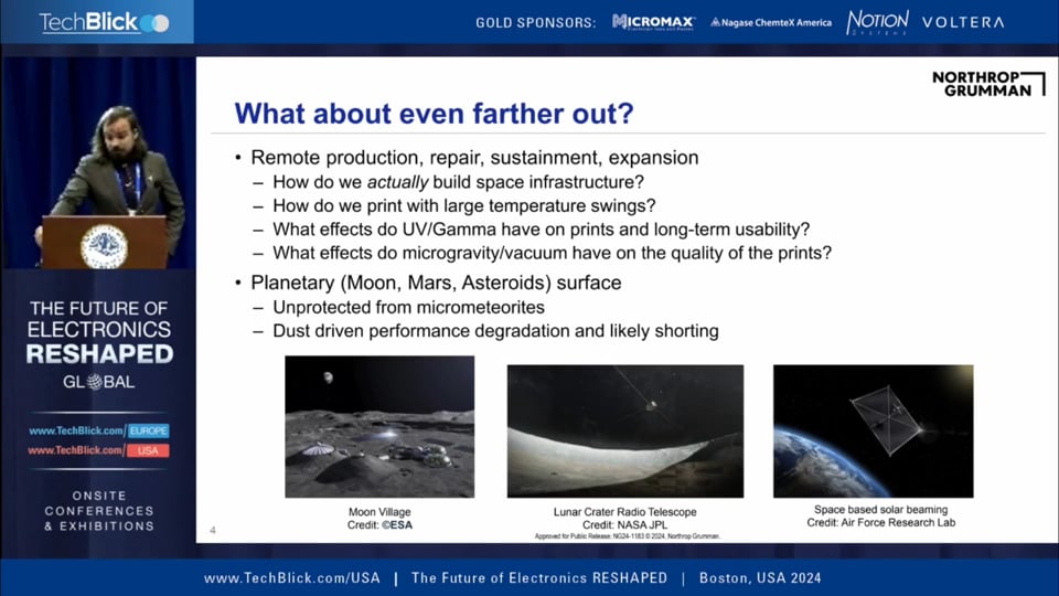
Additive electronics and future of spacecrafts and deployed structured? Watch this video of the talk from Anthony DeCicco how printed sensors are crucial, saving technician time/effort, and how ink technology is becoming reliable and high quality enough for these long lifetime (15+++ year) applications..... Join us at TechBlick USA show on 11&12 June to learn how additive electronics will enable in-space manufacturing. Explore the program here https://lnkd.in/gQKjBZzn 🌌 Monitoring Deployed Space Structures Monitoring the performance of large, deployed space structures over time is a significant challenge, requiring numerous strain sensors across the structure. Solution: Printing sensors directly onto structures could drastically reduce technician time and streamline production. 🖋️ Advancements in Ink Technology Tremendous progress in ink technology and reliability, thanks to efforts by academia and industry consortiums like NextFlex. Focus is shifting toward print quality and long-term reliability for advanced applications. 🚀 Durability for Space Missions Spacecraft components must endure lifetimes of 15+ years, with some geosatellites already surpassing 25 years. Degradation impacts performance, thermal management, and spacecraft operations—making reliability critical. ⚡ Approaching Bulk Conductivity Recent advancements in reactive ink printing have achieved ~85% bulk conductivity, marking a significant step forward. The next challenge: Understanding the effects of long-term usage on these printed components in extreme conditions. 🔭 Future of Spacecraft Production Combining printed sensor technology with high reliability opens doors to innovative, efficient, and long-lasting spacecraft designs.
- R2R printed ultrafine transparent RFID for supply chain management
阿部誠之 from Asahi Kasei explains how their R2R printed ultrafine transparent RFID will be part of a total system including blockchain to enable brand owners to achieve full supply chain management Join us in Boston on 11 and 12 June to learn what more about applications of additive and printed electronics across all sectors. Explore the upcoming program now https://www.techblick.com/electronicsreshapedusa
- The need for R2R and HIGH SPEED printing of perovskite solar photovoltaics?
Thomas Tombs at Energy Materials Corporation explained why at TechBlick 's Future of Electronics RESHAPED show in Boston last here, outlining that the demand will be 75 terawatts of need by the year 2025! Join us on 11 and 12 June again in Boston to RESHAPEE the FUTURE of ELECTRONCIS making it additive, printed R2R, flexible etc. Explore the program --> https://lnkd.in/gQKjBZzn Stephan DeLuca #Perovskites #PrintedElectronics #R2R #Additive #TechBlick #ElectronicsRESHAPED
- Flexible Circuits, E-Textiles, and Wearable Electronics: SSAIL, Graphene Fibers, and Embroidery Technology
This edition dives into the cutting-edge innovations shaping the future of flexible circuits, e-textiles, and wearable electronics. Discover how industry leaders are leveraging technologies like SSAIL, embroidery, graphene fibers, and advanced inks to redefine scalability, durability, and performance across applications. From health monitoring wearables to thermal-regulating textiles, we highlight breakthrough solutions driving adoption in industries such as healthcare, aged care, and fitness. Key topics include SSAIL’s rapid circuit development, Celanese’s stretchable inks, Kyorene® fibers' antibacterial benefits, and embroidery’s automated precision in creating functional textiles. Stay informed on the challenges, advancements, and real-world applications of these transformative technologies. Akoneer | Using SSAIL technology for fast development of flexible circuits RMIT University | Stretchable and flexible electronics reshaped for industry-driven aged-care technologies Celanese | Time to Think Beyond Stretch in Wearable Electronics Graphene One | Graphene based functional fibers for clothing and textiles 3E Smart Solutions | Driving Reliability and Scalability in E-Textiles and Wearables via Embroidery Technology The Future of Electronics RESHAPED USA is TechBlick's premier event, showcasing the latest innovations in electronics. Join us at UMass Boston on June 11-12, 2025 for an exciting exploration of emerging technologies. You can find more details on the event website here. EARLY BIRD rates are available now Register here TechBlick.com Akoneer | Using SSAIL technology for fast development of flexible circuits Tadas Kildusis | 2023 Selective Surface Activation Induced by a Laser (SSAIL) technology is one of the new methods that can address the challenges in circuit formation on flexible substrates. By adapting laser and chemical plating parameters, SSAIL can be used on a wide range of flexible substrate materials to create high-precision and high-quality circuit patterns with strong adhesion, making it highly suitable for use in the production of flexible electronics. Since SSAIL works on standard dielectric materials (PET, PC, PEN, PI, etc.) and there is no tooling changes between different substrates or designs, it allows fast development of new flexible circuits. The line writing speed of 5-10 m/s is then easily transferred from prototyping to production. In this session, you will learn about: The complete SSAIL process, from laser surface modification to the final product. A comparison of SSAIL with Laser Direct Structuring (LDS). Its compatibility with standard dielectric materials. Rapid prototyping capabilities, delivering samples on new materials within two days. Automotive testing applications. Download the Full Slides Here RMIT University | Stretchable and flexible electronics reshaped for industry-driven aged-care technologies Sharath Sriram | 2023 The convergence of lab-based discoveries and industry-need created reimagined products based on stretchable and/or flexible substrates. Soft electronics made of silicone were translated into a printed technology to create smart bedding products to monitor aged-care residents and improve quality of care. Working closely with manufacturers, the evolution of the technology from stretchable electrodes to a sensor array across a mattress, will be covered. This approach represented a new take on production of electronic textiles. Combining flexible substrates with surface mount components, composite structures have created a category of modular sensing skin patches. Based on clinical need, different sensor combinations have been utilised for aged-care health monitoring, with potential use cases targeted to dementia care and post-operative management. In this session, you will learn about: Cross-Disciplinary Collaboration: How user-centric design, business innovation, and industry manufacturing intersect to create impactful solutions. Wearables, Nearables, and Rapid Diagnostics: Exploring the future of health monitoring technologies. Wearing the Future: Transparent, unbreakable electronics designed for aged-care applications. Industry Collaboration Highlights: REMi® - Nearable: A versatile product for health monitoring, sleep studies, and aged-care applications. Vlepis - Wearable: Advanced solutions for health and infection management, including continuous ECG monitoring. Download the Full Slides Here Celanese | Time to Think Beyond Stretch in Wearable Electronics Saeed Madadi | 2023 Celanese Intexar™ line of Stretchable, Washable inks and films have been the premier materials for transforming materials into smart garments since 2018. Since the pandemic, the adoption of wearable technology has taken off not only in fitness applications but also healthcare. As such the testing requirements and needs have changed since the advent of wearable technology. Learn how the Celanese Micromax™ Electronic Inks and Pastes team has been working with customers and gathering market data to understand the evolution and developing products to meet the new needs of the market. In this session, you will learn about: Intexar Films: Addressing key challenges with commercial TPU. Intexar Fitness and Medical Patch Design: Key design considerations, including the number of print layers required. Ink Development Process: How partnerships drive the creation of new inks to meet market demands. Innovations in Pastes: Improved Ag/AgCl (Silver/Silver Chloride) pastes tailored to market needs. New solvent-resistant pastes—exploring the importance of solvent resistance. New stretchable, washable Ag/AgCl—why flexibility and durability are critical in wearable applications. Download the Full Slides Here Join us on February 11-12, 2024, for the Solid-State Battery Materials , a virtual event by TechBlick. Engage with industry leaders driving innovation in battery technology. Explore the agenda here. Register Now TechBlick.Com Graphene One | Graphene based functional fibers for clothing and textiles Dave Vanek | 2022 Graphene One LLC is the first company to commercialize a family of textile fibers based on graphene. Trademarked Kyorene, the fibers are available in polyester nylon, viscose and UHMWPE as staple fibers and filament. The graphene is produced by Graphene One’s parent company and is converted to graphene oxide and added to the fiber at extrusion. The graphene gives the fibers bacteriostatic, odor control, and thermal regulation properties. Kyorene is now commercial in socks, underwear, denim, sportswear, bedding and more. During this session, you will explore: Commercialization Challenges: Insights into scaling up production and overcoming hurdles such as mechanical exfoliation. Kyorene® Graphene Quality: Strict internal quality control measures. Independent external graphene testing to ensure consistency and reliability. Kyorene® Fiber Portfolio: An overview of the fiber options and their diverse benefits. Commercialized Products and Performance: Antibacterial properties with proven bacteriostatic test results. Thermal regulation capabilities, including cooling mechanisms that enhance comfort. Download the Full Slides Here 3E Smart Solutions | Driving Reliability and Scalability in E-Textiles and Wearables via Embroidery Technology Steliyan Vasilev | 2024 Embroidery technology, once rooted in historic hand-stitched garment design, has experienced a remarkable resurgence with the advent of computerization. Due to its unparalleled capacity for material optimization, embroidery offers textile engineers the ability to precisely place single fibers,yarns, fiber bundles, or even wires in a pre-designed geometry. This precision makes embroidery an ideal candidate for integrating functionality into textiles through sensors, actuators, or electrodes. By enabling the automatic integration of conductive fibers and electronic components into textiles,embroidery technology facilitates the creation of e-textiles. This capability opens the door to a myriad of applications, ranging from ECG and EMS electrodes to capacitive, strain and pressure sensors, and even illumination systems and heating elements.Despite the longstanding development of e-textiles, the realization of market-ready products has been limited by high production costs and poor reproducibility resulting from manual production processes. The high degree of automations of embroidery technology, combined with the scalability enabled by multi-head machines, has revolutionized e-textile production. This automation not only reduces costs but also ensures consistent quality, paving the way for the widespread adoption of e-textiles in various industries. You will gain insights on: Solutions and Benefits: Exploring the applications and advantages of embroidery in e-textile production. PCB Integration and Textile Electrodes: How embroidery supports tailored placement for electronic integration. Tailored Placement of Fibers/Wires/Tubes: Practical uses, including heating elements, illumination systems, and sensors. Download the Full Slides Here The Future of Electronics RESHAPED USA Join us at UMass Boston on June 11-12, 2025 for an exciting exploration of emerging technologies. You can find more details on the event website here. EARLY BIRD rates are available now Register here