Search Results
966 results found with an empty search
- Sustainable Inks, PTC Film Heater Design, Next, Gen Battery Separators, ePaper Advances, Novel Silicone Technology
In this edition, we look into materials science, energy storage, printed electronics, and sustainable display technologies. Joanneum Research introduces Supresil®, a patented technology that optimizes the processing window for platinum-cured silicones (LSR and HCR) without compromising material properties, ideal for 3D printing. Celanese Micromax presents PTC film heaters, leveraging Joule heating and printed carbon pastes for uniform, self-regulating thermal solutions across flexible substrates. AilArian addresses the environmental impact of metal-based conductive inks in biodegradable electronics with a novel magnetic separation technique for recovering silver, promoting both high conductivity and eco-friendliness. Sepion Technologies reveals a new battery separator coating that improves moisture resistance, enhances safety, and reduces manufacturing costs, enabling the use of low-cost cathodes. Finally, E Ink compares ePaper with emissive displays, focusing on energy efficiency, readability, and use cases in retail, public information, and digital signage. Joanneum Research | New inhibition technology for (Pt)-cured silicones (LSR and HCR) to optimise the processing window without changing material properties - Supresil® Celanese Micromax | PTC Film Heaters – Materials, Design and Applications AilArian | Magnetic separation of silver conductive material for fully biodegradable electronics Sepion Technologies | The Next-Generation of Battery Separators Eink | ePaper vs. Emissive Displays The Future of Electronics RESHAPED USA #AdditiveElectronics #3DElectronics #PrintedElectronics #WearableElectronics #FlexibleHybridElectronics #WearableElectronics #SustainableElectronics #ElectronicTextiles 🗓️ 11 & 12 June 2025 📍 Boston, USA 🔗 Agenda & Registration: 🎤 70+ World-Class Speakers 🏢 75+ Global Exhibitors 👥 550+ Participants from Around the World 🔥 Early bird rates expire on 25 April 2025! 💥 Limited-time offer: Get an extra $200 discount with this special coupon! Get your coupon here Joanneum Research | New inhibition technology for (Pt)-cured silicones (LSR and HCR) to optimise the processing window without changing material properties - Supresil® Ulrich Trog Platinum (Pt)-cured silicones are gaining in popularity, emphasising addition curing over traditional peroxide methods. They ensure purity and efficacy, resulting in stronger and more aesthetically pleasing products. However, when curing is initiated by mixing parts A and B, the pot life is limited (minutes to hours) depending on the type of silicone and temperature. This creates practical and technological constraints such as short processing time, manufacturing waste, difficult reproducibility, and inflexible manufacturing processes. Our patented formulation extends pot life through reversible inhibition of crosslinking. Unlike systems with state of the art inhibitors our inhibitors evaporate readily and completely once processing begins, even at temperatures below 80 °C, allowing normal cross-linking at mild temperatures for rapid and complete curing while maintaining the original material properties. The benefits of using Supresil® are reduced production costs, ensuring constant production quality and enabling 3D printing. Download the full presentation here Celanese Micromax | PTC Film Heaters – Materials, Design and Applications Andree Maindok Electrical resistance heating is an efficient way of applying heat directly to the surfaces requiring it. Also referred to as Joule heating, such devices can take many forms. Printed conductive inks and pastes present a versatile approach to apply heater patterns and electronic circuitry onto a variety of substrates materials like metals, textile fabrics, rigid and stretchable polymer films, leather and many more. Providing uniform heating power over a large area efficiently directs the heat to the intended surface without the need for heat spreaders or padding to prevent the heater being seen or felt. The heating elements can be printed with fixed resistance pastes, or positive temperature coefficient of resistance (PTC) paste can be used to reduce power as operating temperature is achieved and to reduce overall power consumption. What you will learn from this presentation: PTC – Power as a Function of Temperature: All PTC heaters work on the principle of Joule Heating, where electrical current flowing through a resistor generates heat. PTC Carbon Pastes – Where Do We Stand? A look at the range of sheet resistivities available today for both low and high voltage power supply applications. Features & Benefits – No Thermal Runaway: PTC heaters self-regulate, making them safe and efficient with no risk of overheating. Design Considerations: Understand the dynamics of your PTC heater through powered cycling tests and other assessments that help optimize performance Download the full presentation here AilArian | Magnetic separation of silver conductive material for fully biodegradable electronics James Claypole There is a strong desire to remove plastic from printed electronics; both removing plastic as a substrate and also replacing FRPs in traditional PCB assemblies, including many biodegradable alternatives. The challenge then becomes what happens to the circuit material? Circuits made with carbon-based inks lack the conductivity required for many applications. Metal circuits, such as copper and silver, can accumulate in the environment and reach highly toxic levels or enter waterways. We present our unique solution to this problem, using magnets to recover the conductive material, allowing us to provide inks that are both highly conductive and environmentally friendly. Download the full presentation here The Future of Electronics RESHAPED USA is TechBlick's premier event, showcasing the latest innovations in electronics. Join us at UMass Boston on June 11-12, 2025 for an exciting exploration of emerging technologies. You can find more details on the event website here. Early Bird Registration is now open! Register today and take advantage of our exclusive Early Bird rates before they expire on April 25, 2025 . Special Limited-Time Offer: Get an additional $200 off your registration with our special coupon! 🔗 Get your coupon here TechBlick.Com Sepion Technologies | The Next-Generation of Battery Separators Peter Frischmann Some takeaways from the presentation: Challenges with ceramic coatings: High moisture retention, bulkiness, and limited selectivity. Sepion’s innovation: A next-gen coating that enables low-cost cathodes, requires less drying time, and performs better with less moisture. Enhanced safety & efficiency: Thermo-mechanical stability that matches ceramics with 4x less mass and volume. Download the full presentation here Eink | ePaper vs. Emissive Displays Jonathan Margalit With the growing popularity of electronic Paper (“ePaper”) and the increasing need to deploy sustainable signage solutions, Jonathan Margalit will review the latest advancements in ePaper technology. With the introduction of new color platforms and sizes, Jonathan will discuss the pros and cons of ePaper technology and go over examples of use cases and deployments in retail, hospitality, public information, DOOH, and others, followed by a Q&A session Download the full presentation here The Future of Electronics RESHAPED USA #AdditiveElectronics #3DElectronics #PrintedElectronics #WearableElectronics #FlexibleHybridElectronics #WearableElectronics #SustainableElectronics #ElectronicTextiles 🗓️ 11 & 12 June 2025 📍 Boston, USA 🔗 Agenda & Registration: 🎤 70+ World-Class Speakers 🏢 75+ Global Exhibitors 👥 550+ Participants from Around the World 🔥 Early bird rates expire on 25 April 2025! 💥 Limited-time offer: Get an extra $200 discount with this special coupon! Get your coupon here TechBlick.com
- Innovations Tour in Additive Electronics: From Analog to Digital Printing | Fineline, high viscosity, and 3D
In this article, we highlight a number of printing process innovations that are advancing the state of the art in printed and additive electronics and are addressing critical existing limitations to open new opportunities. Here, we will go on a quick tour from analog screen printing to digital printing to ink-less laser printing. In this journey, we will make many short stops covering screen printing, capillary printing, inkjet printing, EHD printing, micro-dispensing, LIFT printing, dry printing and beyond. Wit over 25 images, tables, charts as well as 13 videos, we cover the following points Screen printing: State of the art ultrafine line printing High production speed in screen printed metallisation Rotary screen printing for PV metallisation Alternative PV metallisation methods (1): Capillary printing Digital printed electronics/additive electronics Can we scale up inkjet printing in functional printing? How to digitally print high viscosity pastes? Digital multi-material laser printing of high viscosity pastes in printed electronics and electronics manufacturing High viscosity digital printing AND ultra fine resolution well beyond inkjet or LIFT Digitally printing higher viscosity levels at ultrafine resolution without e-field? High Pressure Capillary Printing - high resolution, high aspect ratio and high viscosity printing without e-fields, satellites or splashing? Printed Electronics / Additive Electronics without inks? SSAIL Process: Additive laser-induced metallisation of "diverse" surfaces Dry (Ink Free) multi-material direct laser printing To learn more about the wonderful world of Additive and 3D Electronics , join us and 550 others from around the world at the Future of Electronics RESHAPED conference and exhibition in Boston on 11 and 12 June 2025. This is the largest and the most important event in the US dedicated to Additive and 3D Electronics, bringing together over 550 participants, 70 talks, and over 75 exhibitors. Explore here https://www.techblick.com/electronicsreshapedusa Major Early Bird Ends on 25 April. Go HERE to receive a coupon offering you 200 USD additional discount on top of early bird rates. Screen printing: State of the art ultrafine line printing First let us start with one of the largest applications of printed electronics: photovoltaic metallisation. In fact, this application is so large that according to projections this market alone will end up requiring amounts of silver in excess of 100% of the current worldwide silver supply soon, meaning that silver shortage will constrain growth if technological changes do not address the issues. In PV metallisation screen printing has been completely dominant despite many attempts to introduce alternatives. Here, screen printing is the state of the art, pushing the boundaries of what is considered possible every year. The chart below shows the research level progress in ultrafine screen printing in photovoltaic metallisation. It shows that the state-of-the-art linewidth at research level went down from 80-10 µm in 2008 to 17µm or so now. This is an incredible rate of progress and learning. Sources:. Tepner & A. Lorenz, „Printing technologies..”, Progress in Photovoltaics, 2023 But the progress in fineline screen printing is not limited to just research. The industry has actually followed too given the strong need to print ever narrower lines without efficiency loss to reduce silver consumption per cell or watt. This is shown in the chart below which TechBlick has compiled from years of ITRPV roadmaps. The chart shows linewidth of screen printed metallisation as a function of year, demonstrating that the linewidth in mass production has gone from some 90 µm or so in 2012 to now 25 µm. This is just an incredible advancement of the art of screen printed electronics. This achievement is the result of real team effort between printers, screen and mesh makers, paster makers and equipment manufacturers. Sources:. TechBlick compilation from ITRPV roadmap data Below you can see an example from Fraunhofer ISE showing how they managed to improve the topography of the printed lines, making them ever narrower with an aspect ratio of 1. This progress is the result of years of hand-in-hand effort in paste optimisation (rheology, particle size, wall slip, etc), mesh technology (e.g., towards ultrafine 520-11 stainless ones), and emulsion-over-mesh (EOM) technology (e.g., laser opening of EOMs with sub 20 µm openings and ultra long life (80k-100k) print runs in PI), etc Sources: Fraunhofer ISE. Taken from a talk given at the Future of Electronics RESHAPED Berlin 2024 To learn more about the wonderful world of Additive and 3D Electronics , join us and 550 others from around the world at the Future of Electronics RESHAPED conference and exhibition in Boston on 11 and 12 June 2025. Major Early Bird Ends on 25 April. Go HERE to receive a coupon offering you 200 USD additional discount on top of early bird rates. High Production Speed in Screen Printed Metallisation But in this business of PV metallisation, it is not just the linewidths that are impressive, the production speeds and throughputs are also very impressive. As an example, below you can see a printer by Suzhou Maxwell Technologies Co., Ltd. in action. This is a new half-cell TOPCon printer. The parameters are reported in the table below, showing that this equipment can achieve 14400 pieces per hour at half cell at printing speeds of 490 mm/s and a cycle time (CT) of >1s with minimal breakage. This is impressive! Source: Suzhou Maxwell Technologies Co., Ltd. presented at the online TechBlick Screen Printing workshop in 2023 Source: Suzhou Maxwell Technologies Co., Ltd. presented at the online TechBlick Screen Printing workshop in 2023 Below you can also see a full turn-key automatic line for full-size wafers. This data is also from Suzhou Maxwell Technologies Co and was presented at TechBlick in 2023, so is already 2 years old and still impressive! Rotary Screen Printing In production everyone uses flatbed screen printing. But can one also utilise rotary screen printing whilst meeting the linewidth and aspect ratio requirements? Here you can see an example from Fraunhofer ISE again showing a rotary screen printing line which can achieve in a single printing line some 8000 SHJ wafers per hour with a cycle time of just 0.45s at a linewidth of 50um or so. This is impressive for a demonstrator full system machine although it is not yet commercial. In general, given the exacting linewidth requirements and the current status of flatbed screen printing systems, rotary screen printing will not find it easy to go from pilot to production in this application. Rotary screen printing for SHJ PV metallisation. Source Fraunhofer ISE presented a Future of Electronics RESHAPED Berlin 2024 To learn more about the wonderful world of Additive and 3D Electronics , join us and 550 others from around the world at the Future of Electronics RESHAPED conference and exhibition in Boston on 11 and 12 June 2025. Alternative metallisation methods (1): Parallel dispensing Many alternative processes have long sought to replace or at least dent the dominance of screen printing. Here I want to highlight some interesting approaches being developed by the community. First example is from Highline Technology which uses parallel dispensing or homogenous extrusion of metallisation pastes through parallel nozzles. The image below shows the paste being extruded outside the nozzle, and the video below shows the printing process at a pilot equipment. This is an interesting process because it is non contact and can achieve finger widths down to 20 µm with good print speeds exceeding 500 mm per second. Source: HighLine Technology presented at TechBlick online 2023 Furthermore, this printing process can yield nice printed lines with excellent aspect ratios. This is shown below. The left images show printed aluminium traces whereas the right one shows silver lines with a linewidth of 17 µm and a good aspect ratio. Alternative PV metallisation methods (1): Capillary printing Another innovative approach is using capillary printing under pressure. We will come to capillary printing again in another context later in this article. Here the capillary, made out of glass with a narrow 20 µm opening, is brought close to the surface and atmospheric pressure (10 mbar to 11 bar) is applied, pushing the paste out, thus printing at speeds up to 500 mm/s. The process is schematically shown below. You can see also some print profiles, showing the capability to achieve ultra narrow line with good aspect ratio. Here Ag NPs inks are used since larger particles could clog the glass capillary. When applied to a single heterojunction cells the process could achieve 12 µm lines with 6.4 µm height, resulting in a good SHJ efficiency of 22.96%. Critically, this process could lead to 60% less silver consumption. These are impressive results. However, this is relatively early stage and much work needs to be done on parallelisation and on achieving stable print runs. Digital printed electronics/additive electronics Now lets switch from analog to inkjet and DIGITAL printing. The most traditional digital printing method in printed electronics and additive electronics is inkjet printing (IJP). In fact, IJP sets the reference point, and many innovations and developments covered in the rest of this article seek to address the shortcomings of IJP, such as IJP's inability to handle high viscously pastes or its limited print resolution. Can we scale up inkjet printing in functional printing? One common question has always been whether one can really scale the size of inkjet printers when it comes to functional printing. As seen in the image below, the answer is YES! Below one can see a huge inkjet printer - by Kateeva - able to print on Gen 6.5 glass (925x1500mm2) glass. To appreciate the size of the system, it is instructive to see the human next to the machine in the image! This is a commercial system used in production of multilayer encapsulation layers in OLED displays where the organic layer in the barrier is inkjet printed. It is thus area printing and not pixel printing. The video below also shows how the printing actually works, showing the movement of the print heads as well as that of the glass floating on gas. This is an incredible feat of engineering in inkjet printing millions and millions of droplets over huge areas in a production setting. Video presented at the TechBlick Future of Electronics RESHAPED USA in Boston (2024) How to digitally print high viscosity pastes A major shortcoming of IJP has always been its inability to print high viscosity materials. There are many approaches to enabling digital printing of high viscosity materials like screen printable pastes, adhesives, solder, and many other materials. An interesting approach has been taken by Quantica. An example of their print system is shown below. They essentially build a powerful actuation system within the print head able to push out even high viscosity materials. The parameters are shown below. The print head can handle pastes with viscosity levels up to 240 centipoise that have a high loadings (>75 wt%) and even large particulate fillers (5um or so). Thus this print head can open up jetting to all manners of higher viscosity materials including screen printable pastes. Quantica print system showing the print head as well as the actuation and circulation system for printing high viscosity materials in printed electronics Parameters of the Quantica jetting head including operation temperature, nozzle pitch, frequency, nozzle count, etc There are however a couple of challenges that still hinder rapid and widespread adoption in printed electronics. The first is the need to have custom-made pastes necessitating a close collaboration with ink/paste makers who are willing to make such custom formulations. This is because the print head operates at 80C or so. This would mean that most standard screen printing pastes would already begin to dry in the print head and within the circulation system, limiting print runs and stability. This can be addressed with special paste formulation, however. The second current challenge is the limited number of nozzles per print heads. This is the consequence of the fact that the actuation mechanism takes up real estate in the print head design, inevitably limiting the number of possible nozzles. Digital multi-material LASER printing of high viscosity pastes in printed electronics and electronics manufacturing? Another interesting process enabling digital printing of high viscosity pastes is the LIFT (Laser Induced Forward Transfer) process. The operation principle is explained nice in the below video by Coatema. The process works by first coating the paste on a transfer film. A laser then run across the transfer film causing the coated material to be released at points which are laser illuminated. The released materials then land onto the target substrate. Thus the process can digitally with the help of a laser essentially print the material! It can even be done R2R! Interestingly - as shown in the table below - this method can print materials with a wide range of viscosities, ranging from 500 to over 300 000 centipoise. Indeed, in the table you can see that LIFT can print carbon pastes, ceramic pastes, metal pastes, solder, silicon, and even epoxy! The print resolution can also be as low as 40um, thus being comparable to the very best-in-class advanced screen printers found at most contract manufacturers in the printed electronics and electronics manufacturing operations. Table by io-Tech presented at TechBlick's Electronics RESHAPED event in 2023 in Berlin. Below you can see the solder printing in operation by an io-Tech LIFT printer machine. It can print T6 solder at 120 um and T9 at 45um, operating at 5 million drops per hour (equivalent to some 13888 drops per sec). This is thus a high speed and high resolution process able to handle a wide range of viscosity levels. What is unique is that in the same print run - by controlling the laser profile - one can print two different profiles. See the example below. These were done in the same print run! This opens up some nice possibilities. LIFT printing example showing that two different print profiles of solder can be achieved in the same print run. io-Tech presented this at TechBlick Berlin 2023 Interestingly this process also be made R2R. This is explained by Coatema, which is developed such a system, capable of printing on 180mm wide substrate at print speeds of 2-10 m per min and resolutions of up to 600 dpi. Key innovations here will also include ink recycling as well as rapid laser drying, which is more digital and energy efficient than general overn curing (but less flexible and more material specific). This will open up the way for digital and roll-to-roll mass production on flexible substrate. This is important because previous attempts with inkjet printing were not always successful due to limited material menu and process instability Here it is important to mention that ink recycling is crucial. This is because only a small fraction of the paste coated on the transfer film will be printed. Thus - without recycling - the process will be extremely wasteful with a poor material utilisation, which will increase costs, potentially rendering it unviable. Thus this is an important process innovation. High viscosity digital printing and ultra fine resolution well beyond inkjet or LIFT? Thus far we have seen that it is possible to digitally print high viscosity materials. But both mentioned processes have low to moderate resolutions. We will now showcase a range of printing techniques that enable ultra high resolution printing of even high viscosity materials. The first process is EHD (Electrohydrodynamic) Printing. Here, an electric field build into the print head is used to pull out the ink and particles. Thus it is not a classic push process as in inkjet printing. This means that EHD printing can handle much higher viscosity levels and can have narrower nozzles with more focused jets leading to higher resolutions. The schematic below by Scrona shows the design of a multi-nozzle print head showing that each nozzle could be ca 200um wide with its own well-controlled e-field. Scrona multi-nozzle EHD printer heads for printed electronics and QD printing shown at TechBlick conference This process can print with resolutions of 500nm or handle materials with viscosity levels over 10 000 cP. The video below - also by Scrona shown at a TechBlick event - shows the printing of quantum dots (QDs) with a multi-nozzle print head (I think this is a 128 nozzle printer!) A key innovation here is how to scale to multi-nozzle printing. Scrona has developed its own MEMS technology for this together with custom made drive electronics, ensuring small sized multinozzle printer heads with little nozzle-to-nozzle electric field interference process can also handle high viscoisty materials. As shown below, the print head may need to be adjusted, for example, by having wider nozzles. This way it can even print adhesives as shown in the video below (both schematic and video are from Scrona) Can we digitally print higher viscosity levels at ultrafine resolution without e-field? Micro-dispensing offers such a capability. This process - developed by XTPL - is shown in the video below. Here it can be seen that it can not only print ultrafine lines but also do so over 2.5D and 3D surfaces with steep steps, demonstrating the strengths of this process. The chart below shows the market positioning of this process, indicating that it can also go where others can not, namely ultra high viscosity (10 000 to 1 000 000 cP) with a few micrometre resolution, enabling the printing of dense, high viscosity materials at ultrafine resolutions. Indeed the pictures below also demonstrate this, showing printed structure over 3D (over steep steps) at a few micron linewidth resolutions. One question about this process has long been about print speed and productivity since here the print head hovers very close to the substrate often covering only a small area. However, as can be shown below the process is able to print fast at speeds of 8.3 dots per second. This indicates that the process can be industrialised with multiple parallel heads printing at high speeds. High Pressure Capillary Printing - High Resolution, High Aspect Ratio and High Viscosity Printing Without e-Fields, Satellites or Splashing? Another interesting process is the High Pressure Capillary Printing (HPCaP). Here the ink leaves under pressure a resonating pipette with a narrow opening which is vibrating very close to the surface - similar to an AFM system. As shown below, the technology can achieve sub-micron printing resolution and can handle high viscosity pastes up to 100 00 cPa. The technology does not use e-field and causes no satellite or splashing since print head is very close to the surface In the image below you can see an example of a printed line, showing that it can print narrow linewidths as well as narrow pitches. The narrow pitch printing is important, demonstrating control of the print head and high control of the printed material without splashing or satellites You can see below the printing process in action. Here a micro bump is being printed. This is a unique ability because in a single print run the process can print the entire micro bumps with high macro-scale height. This ability to reach macro-scale heights with micron-scale linewidths/diameters is unique amongst most printing processes. The process is rather slow however it still offers some unique value propositions even in this application. In R&D settings, it is much quicker to print micro-bumps and similar structures than go through a complex photolith process. In repair this process is also be unique especially if high aspect ratio printing is involved which most other printing processes can not handle. Printed Electronics / Additive Electronics Without Inks? Additive electronics is somewhat broader than printed electronics in that it includes techniques which are ink-free. Here we want to showcase two innovative laser-based and ink-free additive electronics processes: SSAIL and the NanoPrintek Process. They offer additive (or semi additive) way of manufacturing electronics SSAIL Process: Additive laser-induced metallisation of "diverse" surfaces SSAIL stands for selective surface activation induced by laser! This is a unique process - developed by Akoneer in the laser hotspot of Europe, Lithuania - enabling metallisation of diverse surfaces. This is important because traditional LDS (laser direct structuring) is limited to a narrow set of specially prepared materials containing conductive particulates near the surface which can be exposed by laser illumination. In SSAIL however, the process is not limited to such substrate and can be applied to glass, FR4, ceramics, and a range of materials. The process is shown below. Here, the laser is applied onto the blank surface to create a pattern. A chemical process is then used to active the surface of the laser exposed areas. Finally, those activated areas are electroless plated to form the final part. The process parameters are also shown below. The traces can be typically around 10um (down to 1um also possible), high laser write speeds at 3m/s @10 um, rapid electroless plating, mild process temperature, etc. Below you can see three selected examples. All are made by Akoneer. 1) a fan-out Cu circuit on PI substrate with fine features, 2 ) 15um traces on a standard FR4 substrates, which is a sensitive substrates and demonstrate viability for PCB manufacturing, 3) 10um/10um Cu lines on glass These applications show applicability to a wide range of substrates. They also demonstrate fineline capability. All these via an additive process with properties of electroless plated copper (vs those of conductive inks) Dry (Ink Free) Multi-Material Direct Laser Printing The final process we wish to highlight in this article is a novel dry ink-free multi-material printing process. The process is developed by NanoPrintek. It is shown below. A solid target is inserted into the machine. The laser then ablates the material, forming nano particles which are then directed onto the substrate via nozzles. A sintering laser sitting below the print head then sinters the material. The process does not involve inks and offers a high diversity of material options. The sintering and print steps happen at the same time. It is disruptive in the sense that it takes the ink our of the additive electronics / printed electronics process. Below you can see various examples including 1) printing Cu on FR4 substrates 2) printing tungsten which is very hard to print via ink format 3) printing platinum which is very hard to print via ink format The smallest nozzle is currently 100um but other nozzles are available too (150, 200, 300 and 350, 400um). In the near future, it is hoped that with aerodynamic focusing 20um effective nozzles and thus printed linewidths can be achieved. These are single aperture nozzle at the moment, but work is ongoing on multi nozzle system. Here the particle generated can be cranked up and the generated particles distributed through the multiple nozzle systems. The system can achieve (as limited by nozzle diameter currently) 100um linewidth. It prints layer by layer. The printed layers are typically 200nm so to print thicker lines multiple print runs are required. This can be a limitation in many application where a relatively high current carrying capability is required thus thick paste printing will still make sense. The work space is around 8inch by 8inch today. The achieved conductivity today - without any sintering optimisation - is around one order magnitude below bulk. With optimisation of sintering, it is expected to approach bulk since pure metals are being printed. Note that the sintering laser is below the print nozzle which means that sintering occurs at the same time as the print. The print speeds are up to 20mm per second. It is thus to be compared with other digital processes in productivity and not with the likes of screen printing which are much faster in printing in the same pattern on an industrial scale. To learn more about the wonderful world of Additive and 3D Electronics , join us and 550 others from around the world at the Future of Electronics RESHAPED conference and exhibition in Boston on 11 and 12 June 2025. This is the largest and the most important event in the US dedicated to Additive and 3D Electronics, bringing together over 550 participants, 70 talks, and over 75 exhibitors. Explore here https://www.techblick.com/electronicsreshapedusa Major Early Bird Ends on 25 April. Go HERE to receive a coupon offering you 200 USD additional discount on top of early bird rates.
- Repairing Open Defects in Semiconductors: A Key to Sustainable Manufacturing
The Evolution of the Semiconductor Industry and Its Path to Sustainability Author: Elisa DUQUET, Hummink, elisa.duquet@hummink.com The semiconductor industry is one of the most complex, dynamic, and technologically advanced sectors in the world. It plays an essential role in shaping modern life, serving as the foundation for everything from smartphones and MRI machines to kitchen appliances and space shuttles. In today’s digital world, nearly every device we rely on is powered by semiconductor chips. The demand for semiconductor chips has reached unprecedented levels. According to the Semiconductor Industry Association (SIA), the industry shipped a record of 1.15 trillion semiconductor units last year, this figure means that every person on earth could receive over 150 chips annually. In addition, the SIA announced that the global semiconductor sales hit $627.6 billion in 2024, an increase of 19.1% compared to 2023. The semiconductor industry is projected to reach over $726.73 billion by 2027. We are Exhibiting! Visit our booth at the TechBlick event on 11-12 June 2025 in Boston . Contact us for your special discount coupon to attend (elisa.duquet@hummink.com) As production scales up to meet increasing demand, so does the need for sustainable solutions to manage waste and defective components. Indeed, the twelve largest semiconductor manufacturers together generate about 2.7 million tons of waste annually - about as much as 5 million EU citizens. Nearly 50 percent of the waste generated by the semiconductor industry is classified as hazardous (V.A. Heinrich & D. Hübner). This waste includes defective or obsolete chips discarded during manufacturing. In the worst scenario and without further proactive measures, the amount of waste could almost double by 2030, due to expected production growth. Figure 1: High aspect ratio bumps, printed by HPCaP with silver ink Historically, the semiconductor industry has focused on relentless innovation and mass production, often leading to significant electronic waste and the rapid obsolescence of components. However, a transformative shift is occurring - one that prioritizes repair and sustainability. In the semiconductor industry, several printing methods can be used to correct production defects and reintegrate components into production lines. These techniques primarily aim to restore defective interconnections and repair open defects at the RDL or bump level. Inkjet printing enables material deposition using an inkjet process without having contact with the substrate. This method minimizes the risk of substrate damage, but it offers limited precision (>10 µm in line width). EHD (Electrohydrodynamic) printing, on the other hand, uses electric fields to generate droplets and deposit conductive inks. However, this technology is complex to implement, as reproducibility becomes challenging at high resolution and requires precise control of electrical parameters. Finally, UPD (Ultra-Precise Deposition), which applies pressure, is also limited in terms of resolution. Indeed, the pressure applied tends to expand the deposits. To overcome the challenges of existing techniques, HPCaP technology introduces a breakthrough approach, enabling ultra-precise, high-resolution repairs that ensure superior electrical performance and seamless reintegration of semiconductor components into production lines. Figure 2: Pads printed by HPCaP, with silver ink HPCaP technology: Correcting Production Defects for Semiconductor The HPCaP (High Precision Capillary Printing) technology, developed by Hummink, offers an innovative alternative to traditional additive manufacturing methods. Based exclusively on capillary forces and resonance, HPCaP technology allows for a remarkable level of precision in depositing various materials. HPCaP technology offers effective repair of production defects at the level of RDLs, flip chip bumps, and interconnections in order to improve the yield and put the chips back into production lines. We are Exhibiting! Visit our booth at the TechBlick event on 11-12 June 2025 in Boston . Contact us for your special discount coupon to attend (elisa.duquet@hummink.com) Unlike other conventional repair methods, such as inkjet printing or chemical vapor deposition (CVD), HPCaP achieves an exceptionally low resistivity of less than 10 µΩ·cm, ensuring optimal electrical performance. Additionally, with HPCaP a resolution of less than 2 µm (L/S) is feasible, providing the means to correct RDLs at the needed submicron scales with high precision and reliability, overcoming a key challenge in semiconductor repair. Beyond RDL repairs, HPCaP technology is also effective in addressing missing bumps - a common production defect in advanced packaging. HPCaP provides a solution that meets the new industry specifications by creating high aspect ratio bumps (up to 20:1) and microbumps of diameters less than 5 µm; all while maintaining excellent resistivity and ensuring both high reliability and reproducibility. Furthermore, HPCaP technology allows for the repair of missing interconnections and damaged pads, restoring semiconductor functionality without requiring costly replacements. By enabling precise, high-performance production repairs, this technology allows semiconductors to be put back into production lines and improve their yield, supporting a more sustainable approach to microelectronics manufacturing. Figure 3: Conductive silver lines printed with HPCaP Conclusion Innovation and sustainability must be combined as the semiconductor industry is at a pivotal crossroads. As demand for semiconductor chips continues to grow, so does the urgency to adopt environmentally responsible practices that mitigate waste and extend the lifespan of electronic components. Repairing, rather than replacing, defective semiconductors is a crucial step toward achieving this goal. HPCaP technology offers an efficient and high-performance alternative to traditional methods in terms of precision semiconductor repair. By enabling the restoration of open defects, missing bumps, and damaged interconnections with unparalleled accuracy, HPCaP not only enhances yield and efficiency but also significantly reduces electronic waste through the production line. Companies that invest in cutting-edge repair technologies like HPCaP will not only gain a competitive advantage but also contribute to a greener, more responsible future for microelectronics manufacturing. The shift toward sustainability is no longer optional - it is the key to long-term resilience and progress in the semiconductor industry. We are Exhibiting in Boston and Berlin. Visit our booth at the TechBlick event on 11-12 June 2025 in Boston 22-23 October 2025 in Berlin Contact us for your special discount coupon to attend (elisa.duquet@hummink.com)
- Saralon | New Ink Sets for Stretchable Printed Electronics Applications
Author: Steve Paschky Saralon now offers new ink sets for stretchable membrane switches, heaters, and electroluminescent display printing. Each of these sets contains all the essential ink components tailored to each application, simplifying your work for a seamless, high-quality experience. We are Exhibiting! Visit our booth at the TechBlick event on 11-12 June 2025 in Boston Last year, I wrote about our range of stretchable Saral Inks , designed for different substrates with various formulations like silver, carbon, and others. Since then, technology has continued to evolve, and so have the needs of the industry. We’ve been hearing from customers that they need stretchable inks that are not only conducting but also provide features like heating and capacitive touch, all while withstanding dynamic forces like bending, stretching, and twisting. One of our major focuses at Saralon has been on providing "ink sets"- collections of compatible inks that are designed for specific applications of Printed Electronics (PE). This approach aligns with our company’s mission: Simplifying Electronics Through InkTech. PE devices often require printing multiple layers of ink on top of each other, and one common challenge for developers is finding the right combination of inks that work well together. That’s where our Saral Inks Sets come in. For specific PE applications, we offer complete sets of inks that are compatible with one another, easy to print, and ensure a trouble-less printing process. For instance, we introduced SaralBattery Inks , SaralEC Display Inks , and SaralEL Display Inks few years ago; designed for printing batteries, electrochromic displays, and electroluminescent displays on flexible substrates. As the demand for stretchable electronics has grown, it was clear that we needed to develop new stretchable ink sets that go beyond just conductivity and provide specific functionalities for particular applications. And that’s exactly what we’ve done. This year, we’ve launched new ink sets for stretchable heaters, membrane switches, and electroluminescent displays. Ink set for printing heaters on stretchable materials Applications like surface heating in automotive, specially on complex geometries like arm rest areas demand printed electronics heaters that can easily stretch and twist. The other application areas include therapeutic and medical devices, hospit al equipment like blankets and bed components. Stretchability offers more comfort, easier integration into product, and higher reliability under dynamic forces. Saral StretchHeater Inks Saral StretchHeater Inks Saral StretchHeater Inks contains all three ink components needed for printing stretchable heaters. Saral StretchSilver 100 is the silver based conductive ink that offer over 300% stretchability with a sheet resistance of 30mΩ/sq/25 μm. It is screen printable and thermally dried at 90°C – 130°C. Saral StretchCarbon 200 is the carbon based stretchable electrically conducting ink, suitable for printing on different stretchable surfaces e.g. TPU. We recommend a drying temperature of 120°C to reach a sheet resistance of 60mΩ/sq/25 μm. Saral StretchDielectricT 300 is a solvent based stretchable, transparent dielectric ink, suitable for elastic substrates. The ink is suitable as a protective layer on top of stretchable silver layers. The ink is screen printable and we recommend a curing temperature of 120°C. Saral StretchMembrane-Switch Inks Ink set for printing stretchable membrane switches Be it in white goods, HMI, car interiors, etc. creating three dimensional (3D) capacitive touches offers a completely different level of design freedom and user experience. For such purposes, we’ve developed a complete stretchable ink set. Saral StretchMembrane-Switch Inks includes all needed ink components for printing membrane switches on stretchable substrates like TPU. The Silver and Carbon ink components, are basically the same inks that are used in printing stretchable heaters, namely: Saral StretchSilver 100 and Saral StretchCarbon 200. For the Dielectric part however, we’ve developed an UV curable ink. Saral StretchUVDielectricG 100 is the UV curable and stretchable dielectric ink, suitable for elastic and flexible substrates. The ink is with green pigment and up to 100% stretchability is possible. Print Stretchable Electroluminescent Displays Ink set for stretchable electroluminescent printing. While we already have a standard ink set for EL display printing on common PE materials e.g., plastic and paper, there is still demand for stretchable EL displays for applications like 3D backlight design, that’s why we have a full set of inks for stretchable EL printing. Saral StretchEL Display Inks contains four ink components and comes with AC/DC inverter. Again, the conducting silver ink is our high-performance Saral StretchSilver 100 with the specifications that were mentioned above. The three other stretchable ink components are as the following. Saral StretchDielectricW 200 is a Barium Titanate based stretchable dielectric ink, suitable for elastic substrates and offers ~ 100% stretchability. Saral StretchPhosphor 100 is the stretchable light emitting electroluminescent ink that comes in blue, orange, white, and green colors. Saral StretchTCPolymer 100 is the transparent conducting ink offering over 300% stretchability on various elastic substrates. These new Saral Inks Sets are designed to support PE developers across a range of industries, including automotive, HMI, surface heating, capacitive touch panels, wearables, etc., offering simplicity in printing, reliable functionality, and design flexibility. They’ve been created based on the input from our partners and clients in the Printed Electronics industry; which plays a crucial role in our development process. We always welcome any further ideas. So, please feel free to get in touch
- Material Innovations: QD color conversion, copper inks for printed electronics, indium solder bumps for microLEDs, battery Safety in Na batteries, and more
Fraunhofer IAP | Quantum Dot Color Conversion in MicroLED – A Material Perspective - Quantum Dot (QD) materials for color conversion in MicroLED displays. Key topics include high quantum efficiency QDs, tailored ink formulations, and EHD-Jet printing techniques for high-resolution applications. The session explores QD stability, ligand optimization, and methods to close the green and red gap in MicroLED displays. Saralon GmbH | Conducting Copper Ink for Printed Electronics: An Application-Based Journey - Saral Copper Ink as an alternative to costly silver-based inks for printed electronics. The session covers copper ink’s stable conductivity, processability via conventional screen printing, and its application in low-cost, high-demand sectors. It highlights challenges and benefits for future electronics manufacturing. INTLVAC THIN FILM | ICARUS: Indium Solder Bump Deposition System- Focusing on improving indium solder bump deposition, addressing pattern hole closure, dendritic growth prevention, and enhancing bump quality. Insights on system stability and reliability for semiconductor assembly and MEMS packaging will also be discussed. Flexoo | Excellence in European Manufacturing: Focus on Contract Manufacturing and R&D Services- Exploring mass-customization in high-end sensing solutions. Topics include the production of BaMoS and MiniMoS sensors, battery behavior analysis at the cell level, advanced wiring solutions, and the role of digitalized processes in manufacturing efficiency. E-Lyte Innovations GmbH | Enhancing Battery Safety in Sodium-Ion Batteries - Addressing the performance challenges of Sodium-Ion Batteries (SIBs), focusing on electrolyte optimization to prevent degradation and sodium plating. The session talks about additive development, test plans for improving efficiency and safety, and a comprehensive review of existing patents and research on SIB technologies. The Future of Electronics RESHAPED USA #AdditiveElectronics #3DElectronics #PrintedElectronics #WearableElectronics #FlexibleHybridElectronics #WearableElectronics #SustainableElectronics #ElectronicTextiles 🗓️ 11 & 12 June 2025 📍 Boston, USA 🔗 Agenda & Registration: 🎤 70+ World-Class Speakers 🏢 75+ Global Exhibitors 👥 550+ Participants from Around the World 🔥 Early bird rates expire on 25 April 2025! 💥 Limited-time offer: Get an extra $200 discount with this special coupon! Get your coupon here Fraunhofer IAP | QD color conversion in MicroLED – a material perspective Manuel Gensler Quantum Dot (QD) materials are emerging as promising candidates for color conversion in MicroLED displays, offering significant advantages over traditional RGB emitting backplanes. The Fraunhofer IAP has developed exceptionally stable QDs with enhanced properties, including high quantum efficiencies under blue illuminance and improved solubility for ink formulation. These advancements are crucial for the practical application of QDs in display technology. Furthermore, the talk will showcase the application of EHD-Jet printing techniques to achieve high-resolution printing of 10 µm and less, even on multi-nozzle systems. This demonstration paves the way for future up-scaling to industrial processes, potentially revolutionizing the manufacturing of MicroLED displays. What You Will Learn from This Presentation: The Green and Red Gap for LEDs in the MicroLED Size (1 – 30 μm) Quantum Dot Color Conversion: The Currently 3 Promising Candidates Printable Quantum Dots for Color Conversion – Tailored Materials and Printing Processes (Ink-Jet, EHD-Jet) Quantum Dot Stability – Optimizing the Ligands Quantum Yield and Stability – Giant-Shell Approach Ink Formulation and Printing – Ink-Jet and EHD-Jet Techniques Devices Increasing the Blue Absorbance & Optimized Encapsulation Download the full presentation here Saralon GmbH | Conducting Copper Ink for Printed Electronics : An Application-Based Journey Steve Paschky Silver based conductive ink is the backbone of the Printed Electronics. However, volatile silver prices necessitate the development of conductive inks with lower cost underlying Materials. Such an alternative must provide comparable conductivity while ensuring stable conductivity levels over time, and easy processability using conventional printing technologies (i.e.screen printing). Introducing a novel low-cost Saral Copper Ink, this presentation guides you through the high-demand application areas, discusses the benefits and addresses how to overcome challenges. Join us in Boston and stop by our booth to learn more! Download the full presentation here INTLVAC THIN FILM | ICARUS: Indium Solder Bump Deposition System Dino Deligiannis Insights you will gain from this session How we minimized pattern hole closure How we improved bump quality by preventing dendritic growth Prevention of spits System stability and reliability Indium bumps we produce Download the full presentation here The Future of Electronics RESHAPED USA is TechBlick's premier event, showcasing the latest innovations in electronics. Join us at UMass Boston on June 11-12, 2025 for an exciting exploration of emerging technologies. You can find more details on the event website here. Early Bird Registration is now open! Register today and take advantage of our exclusive Early Bird rates before they expire on April 25, 2025 . Special Limited-Time Offer: Get an additional $200 off your registration with our special coupon! 🔗 Get your coupon here TechBlick.Com Flexoo | Excellence in European Manufacturing: Focus on Contract Manufacturing and R&D Services Thomas Rohland Key points covered in this presentation Mass-Customization: The Mass-Production of High-End Sensing Solutions — What is Required for Mass-Customization? Outstanding Sensors: From BaMoS to MiniMoS Gain an understanding of battery behavior at the cell level Learn how to monitor pressure distribution within your system/device Versatile Wiring Solutions Explore how wiring lines are gradually shifted within one repetition of the printing cylinder, leading to a shift in the bus connector in the transverse direction with each revolution Technically Advanced Solutions & Gathered Knowledge Discover the benefits of digitalized processes that enable fast processing of customer requests Understand the subject matter and the challenges it presents Download the full presentation here E-Lyte Innovations GmbH | Enhancing battery safety in Sodium-Ion Batteries Jonathan Bäthge The electrolyte plays a crucial role in improving key performance indicators (KPIs) such as efficiency, cost, safety and lifespan of a Sodium-Ion Battery (SIB). By adjusting the electrolyte to prevent active material degradation and sodium plating on the anode, which represent currently occurring problems while cycling SIBs at high cut-off voltages, an enhancement in performance of SIBs can be achieved. Patent and literature analyses were conducted to identify relevant existing electrolyte components, providing a foundation for further electrolyte development and research on new additives. Therefore, new electrolyte additives were investigated to improve the safety and lifespan of SIBs. Key Takeaways from the Presentation Sodium-Ion Batteries (SIBs): Overview of current operational challenges from literature. Patent Analysis: Multi-source approach for patent data collection combined with a Python-based methodology for data processing. Test Plan: Absolute and relative discharge capacity measurements. Post-mortem analysis of battery performance. Archimedes measurements for material evaluation. Download the full presentation here The Future of Electronics RESHAPED USA #AdditiveElectronics #3DElectronics #PrintedElectronics #WearableElectronics #FlexibleHybridElectronics #WearableElectronics #SustainableElectronics #ElectronicTextiles 🗓️ 11 & 12 June 2025 📍 Boston, USA 🔗 Agenda & Registration: 🎤 70+ World-Class Speakers 🏢 75+ Global Exhibitors 👥 550+ Participants from Around the World 🔥 Early bird rates expire on 25 April 2025! 💥 Limited-time offer: Get an extra $200 discount with this special coupon! Get your coupon here TechBlick.com
- Additive and 3D Electronics: LIFT for high viscosity, gravure printing, micro-bump Printing, Cu in Si TOPcon PV, inkjet on 8.5-Gen glass, high viscosity IJP, laser additive process for RDLs, etc
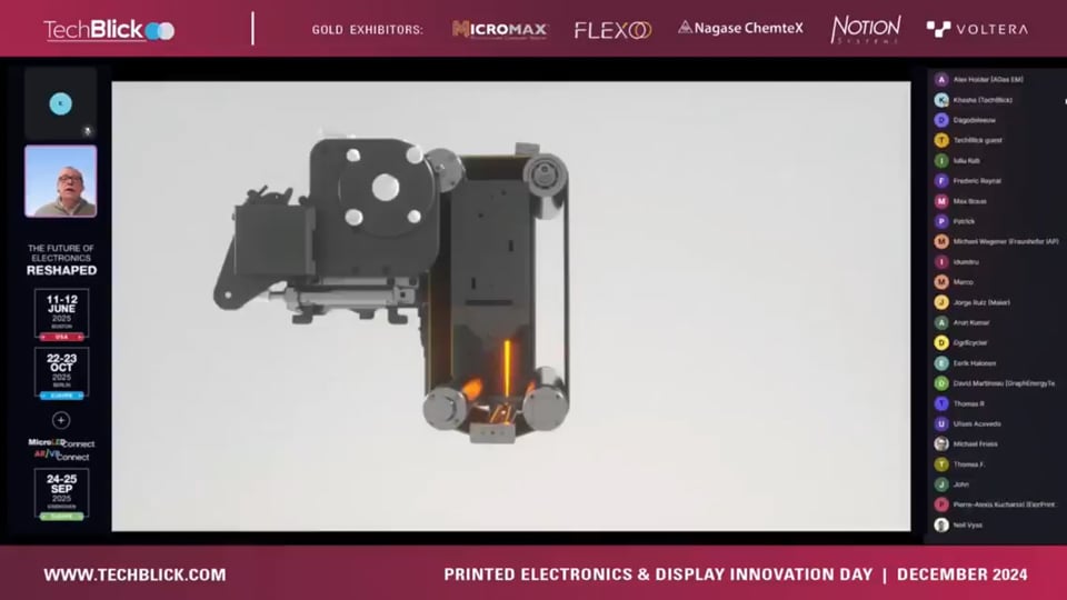
In this newsletter you can learn about the latest advances in Additive, Sustainable, Hybrid and 3D Electronics! via the following highlighted short videos, each being less than 2min, saving you learning time. These are all key points and advances in the field, advancing the art and cutting-edge. LIFT: R2R Digital Printing of High Viscosity Materials | Coatema How does Gravure Printing work in Printed Electronics? | Komori How to print micro bumps in a single step for semiconductor electronic packaging? | Hummink Can copper paste be used in Si TOPCon solar cell metal lisation to reduce silver consumption per cell and per watt ? | ISC Konstanz and Copprint How an actual inkjet printer prints functional and optoelectrical materials on a HUGE 8.5-Gen (2200 x 2500 mm2) display glass? | Kateeva Can we inkjet print screen printable and high viscosity pastes? | Quantica Laser-based additive electronics to simplify the RDL metallization process | Akoneer Time To Explore The World of Additive, Sustainable, Hybrid and 3D Electronics! Join the Electronics RESHAPED USA conference and exhibition in Boston (11 & 12 June) - Where the global Additive and 3D Electronics industry connects. Explore & RESHAPE The Future of Electronics NOW R2R Digital Printing of High Viscosity Materials? This is where inkjet struggled due to requirement for low viscosity inks and also nozzle clogging. LIFT can be a solution enabling R2R digital printing of materials with a range of viscosity levels, finally addressing a key industry limitation? Here in this short video Thomas Kolbusch from Coatema explains how R2R LIFT process works. This is a great explanation so we recommend watching it Video length: 1.5 min How does Gravure Printing work in Printed Electronics? Ever wondered how gravure printing actually works - especially in printed electronics? Hear Doug Schardt from Komori Corporation give a concise 2-min explanation of this wonderful process able to achieve very fine feature with all manners of inks, resists, etc at great scale and throughput. Video length: 2min How to print micro bumps in a single step for semiconductor electronic packaging? High Precision Capillary Printing (HPCaP) developed by Hummink enables the ability to print in a single step micro-bumps with ability to control diameter and aspect ratio. This capability enables amazing applications in semiconducting packaging. In particular, in laboratory and prototyping settings, this can accelerate the development process despite the actual printing step being relatively slow, since it eliminates many process steps. Video length: 1.2min Can copper paste be used in Si TOPCon solar cell metallisation to reduce silver consumption per cell and per watt? If silver consumption per solar wafer remains unchanged, silver shortages will limit the growth of the photovoltaic industry. It is thus vital to switch away from silver or reduce silver consumption. But adding printed copper with the right performance and reliability has been difficult to achieve and demonstrate. Here, ISC Konstanz has demonstrated that YES one CAN use indeed Cu paste with excellent performance AND high stability!! Here you can see the results from Ag consumption has been reduced from 126 mg to 60 mg (with additional of 97mg of Cu as bus bars) with same or higher performance. Furthermore, the solar cells are stabe passing • 3x IEC @ TCT (600 cycles) requirements passed without considerable degradation • 2x IEC @ DHT (2000h) requirements passed without considerable degradation • 3x IEC @ DHT (3000h) requirements passed without any degradation by the group with the encapsulation material EVA Video length: 1.2min How an actual inkjet printer prints functional and optoelectrical materials on a HUGE 8.5-Gen (2200 x 2500 mm2) display glass? Inkjet in printed electronics is often a small desktop machine throwing up the question can it ever be scaled up to huge areas. Here you can see see that yes it can. This is an example of area printing but still a great demonstrator. This video by Kateeva shows this beast of a machine and wonderful engineering in action demonstrating the inkjet can be truly scaled in additive and printed electronics Video length: 30s Can we inkjet print screen printable pastes? Inkjet has this major limitation of not being able to print high viscosity or even mid viscosity pastes. This limitation has truly held back inkjet in the world of additive and printed electronics. Quantica has developed a printer head that could enable direct inkjet printing of high viscosity pastes. This could be a game changer provided some challenges are addressed. Learn more here including about some of the challenges such as drying of paste during print at elevated temperature. Video length: 1.3min Can mask-less Additive Electronics simplify the RDL metallization process (both via and conductor layers) reducing number of process steps from ca. 11 down to 2-4 without any masks? This would be a superb achievement? Tadas Kildušis explains how SSAIL (Selective Surface Activation Induced by Laser) process (PI coat, laser pattern, activate, plate) can achieve this
- Additive Printed Electronics Advances: 3D Additive Lithography, R2R Pilot Line, Micro-Dispensing, Gravure Printed Micro-Bumps, Ultra Fineline Metallisation, Anisotropic Conductive Adhesives
In this newsletter you can learn about the latest advances in Additive, Sustainable, Hybrid and 3D Electronics! via the following highlighted short videos, each being less than 2min, saving you learning time. These are all key points and advances in the field, advancing the art and cutting-edge. R2R pilot hybrid electric manufacturing line for wearable sensors? | VTT What are the real applications of ACFs (anisotropic conductive films)? | CondAlign How is micro-dispensing positioned and how fast can it print? | XTPL How to print silver lines finer than human hair on Si photovoltaics | Fraunhofer ISE How does the 3D additive lithography for additive electronic work? | Holst Centre Why is there a need for direct gravure printing of manufacturing solder bumps? | Komori The Future of Electronics RESHAPED USA Conference and Exhibition #AdditiveElectronics #3DElectronics #PrintedElectronics #WearableElectronics #FlexibleHybridElectronics #WearableElectronics #SustainableElectronics #ElectronicTextiles 🗓️ 11 & 12 June 2025 📍 Boston, USA 🔗 Agenda & Registration: https://www.techblick.com/electronicsreshapedusa 🎤 70+ World-Class Speakers 🏢 75+ Global Exhibitors 👥 550+ Participants from Around the World 🛑🛑 In addition to the early bird rates, there is a special one-time promotion offering an additional 200 USD discount. Get your coupon here . The early bird rates expire on 25 April 2025. 🛑🛑 R2R pilot hybrid electric manufacturing line for wearable sensors? Here you can see the VTT pilot line including pre-cut, bonding and SMT assembly stage. This pilot line - together with the deep expertise to operate the line - is an essential for the development for flexible hybrid electronics and wearable applications, in particular in reaching prototyple and pilot production level. Video duration: 50s #PrintedElectronics #R2RManufacturing #WearableElectroncis #WearablePatches What are the real applications of ACFs (anisotropic conductive films)? ACFs (anisotropic conductive films) are a critical technology in the FHE space. But have you ever wondered what the actual applications and use cases might be? Here, CondAlign AS outlines specific use cases in this short video including biofuel cells, logistic and tracking smart labels, printed segmented OLED displays, and printed electronic signage. Video Duration: 1m46s #Interconnects #SoftToRigidInterconnects #FlexibleInterconnects #LowTemperatureInterconnects #Adhesives #FlexibleHybridElectronics How is micro-dispensing positioned and how fast can it print? Micro-dispensing can achieve both very high resolutions (down to 1um) and handle very high viscosity levels (1 000 00 cP) addressing critical shortcomings of inkjet without requiring an external electric field. Furthermore this technology can also print on 2.5D and 3D surfaces. Here Ludovic SCHNEIDER from XTPL demonstrates examples of printed profiles, showcasing that they can print millions of dots at speeds approaching 10 drops per second for 10 um microdot (micro-bump) printing Video Duration: 30s #MicroDispensing #UltrafinePrinting #3DPrintedElectronics #3DElectronics #BeyondInkjet How to print silver lines finer than human hair on Si photovoltaics? The narrowing of printed metallisation lines to reduce silver consumption per watt is one of the most successful technology development stories in printed electronics, going from 80um or so in 2010 to now 14um in record state-of-art results! But how to achieve ultra fine-line (14um) and high aspect ratio (15um) printed Ag metallisation lines on silicon photovoltaics? here researchers from Fraunhofer ISE show examples of paste optimisation for different screens and also screen optimisation (mesh doubt, opening diameter, etc) to achieve these record results Video Duration: 1m30s #ScreenPrinting #Photovoltaics #Metallisation #FineLinePrinting #StateofArtResults How does the 3D additive lithography for additive electronic work? This is a novel approach developed at the Holst Centre. You can learn how the process work. A key point of this additive lithography is what determines the ultimate resolution of the printed parts, is it the printer or the maskless photolithography of the resin? This technology has use cases in microelectronics and semiconductor packaging Video Duration: 30s #AdditiveElectronics #MasklessLithography #SemiconductorPackaging #Resin #AdditiveLithography Why is there a need for direct gravure printing of manufacturing solder bumps? Here you can learn about the relationship between solder type, particle size, and application including in the emerging area of microLEDs and you can then understand where gravure printing seeks to play. Video Duration: 30s Komori America Corporation #GravurePrinting #PrintedElectronics #MicroLED #AdditveElectronics #MicroBumps #Interconnects The Future of Electronics RESHAPED USA Conference and Exhibition #AdditiveElectronics #3DElectronics #PrintedElectronics #WearableElectronics #FlexibleHybridElectronics #WearableElectronics #SustainableElectronics #ElectronicTextiles 🗓️ 11 & 12 June 2025 📍 Boston, USA 🔗 Agenda & Registration: https://www.techblick.com/electronicsreshapedusa 🎤 70+ World-Class Speakers 🏢 75+ Global Exhibitors 👥 550+ Participants from Around the World 🛑🛑 In addition to the early bird rates, there is a special one-time promotion offering an additional 200 USD discount. Get your coupon here . The early bird rates expire on 25 April 2025. 🛑🛑
- Wearable Neurotechnology, Printed Dielectrics, OTFTs, Jetting Electronics, R2R OPV for Energy Harvesting
Wearable neurotechnology, printed electronics, OTFT displays, and light energy harvesting. Researchers at Stanford University are developing innovative neurosensing and neuromodulation technologies, including fNIRS headbands for monitoring mental states, ultrasound neuro-immunomodulation for treating Parkinson’s disease and stroke, and e-Skin EMG sensors for improved prosthetic control and gait correction. ChemCubed is advancing inkjet printing for multilayer electronics, using ElectroJet™ nanoparticle-free silver conductive ink and high-performance dielectric materials to create advanced circuit boards for capacitors, sensors, and antennas. SmartKem is scaling up its low-temperature OTFT technology for AMOLED and MicroLED displays, leveraging TruFlex™ organic materials that enable flexible, solution-based electronics with low-NRE processing and ULEF integration for ultra-low energy consumption. Epishine is eliminating the need for disposable batteries in connected sensors by harnessing ambient light energy, creating self-charging battery technology that extends device lifespan and reduces environmental impact. Essemtec is optimizing conductive adhesive dispensing for printed electronics manufacturing, improving reliability and efficiency through rheology optimization and jetting technology. Stanford University | Looking ahead – Research topics in wearable neurotechnology innovations from Stanford University ChemCubed | Printing Dielectric Layers in Multilayer/Multimaterial for Additive Manufacturing of Electronics SmartKem | Organic Thin-Film Transistor Technology – from Lab to Fab Epishine | Reimagining the Capture of Light : Innovations in Light Energy Harvesting for a Battery-Free Future Essemtec | Challenges and solutions for jetting in printed electronics The Future of Electronics RESHAPED USA #AdditiveElectronics #3DElectronics #PrintedElectronics #WearableElectronics #FlexibleHybridElectronics #WearableElectronics #SustainableElectronics #ElectronicTextiles 🗓️ 11 & 12 June 2025 📍 Boston, USA 🔗 Agenda & Registration: https://www.techblick.com/electronicsreshapedusa 🎤 70+ World-Class Speakers 🏢 75+ Global Exhibitors 👥 550+ Participants from Around the World 🛑 The early bird rates expire on 25 April 2025. 🛑🛑In addition to the early bird rates, there is a special one-time promotion offering an additional 200 USD discount. Get your coupon here Stanford University | Looking ahead – Research topics in wearable neurotechnology innovations from Stanford University Angela McIntyre Neurotechnology research is making real the possibility of human brain and nervous system activity being measured and altered. Neurosensing can lead to better interfaces with technology, an increased understanding of the effectiveness of medication, and new insights into how the nervous system helps regulate physiology and biochemistry. Neuromodulation is enabling new approaches to therapies for rheumatoid arthritis, tinnitus, stroke, and Parkinson’s disease using wearable devices. An overview of the variety of research at Stanford U. related to wearable eurotechnology will be presented, such as the following examples. Haptic wristbands stimulate nerves to create the perception of grasping an object in VR while leaving hands free. A functional Near-Infrared Spectroscopy (fNIRS) headband is in development for measuring blood flow changes in the brain that correspond to different mental states and may be used for biofeedback to reduce stress. Whereas electrocardiography (ECG) patches on the chest sense signals from the heart and detect arrhythmia, wearable sensors on the abdomen measure contractions of the stomach and gut to model the function of organs and help clinicians diagnose digestive issues. Electromyography (EMG) can be used with biofeedback to help individuals modify their walking gait to reduce long-term knee injury or improve athletic performance. EMG signals for muscles occur before the motion, which may lead to prediction of movement and increased responsiveness for exoskeletons. Arrays of stretchable electrodes on the surface of the skin enable greater EMG precision than discrete electrodes when reading electrical signals. These e-skin arrays potentially lead to smoother control of robotics, feedback when training for delicate tasks, and more realistic interactions in VR. Key insights from this presentation: • fNIRS for determining mental states • Ultrasound for neuro-immunomodulation • EGG monitoring “gut as second brain” • e-Skin electrodes for EMG • EMG for improving gait • Haptics for altering perception • VTS therapy after stroke • VTS therapy for Parkinson’s disease • Plasticity of neural pathways • Acoustic therapy for tinnitus Download the full presentation here ChemCubed | Printing Dielectric Layers in Multilayer/Multimaterial for Additive Manufacturing of Electronics Daniel Slep Dielectric materials play a critical role in modern electronics as they serve as insulators that prevent electrical charges from flowing between conductive parts. In recent years, significant advances have been made in the development of dielectric materials, driven by the demand for improved performance and efficiency in electronic devices. Novel methods have been developed for processing and integrating dielectric materials into electronic devices, including inkjet printing, plasma-enhanced chemical vapor deposition, and self-assembly techniques. These advances have enabled the fabrication of electronic devices with improved performance, reduced size, and lower power consumption. ChemCubed has adopted inkjet printing since it’s a promising technique for the fabrication of electronic devices due to its precision, versatility, and low cost. Together with our commercialized silver ink, we are able to print circuit boards with complex structures for electronic devices such as capacitors, sensors, and antennas, which have potential applications in diverse fields such as healthcare, energy, and communication. Highlights from the session: Key factors to consider when selecting a deposition technology for your application. ElectroJet™ Materials: A nanoparticle-free silver conductive ink designed for high-performance applications. Inkjet-printed electronics powered by ElectroJet™: Multi-layer, multi-material capabilities with eight-channel precision. Introducing our latest innovation—high-performance dielectric ink for next-generation electronic devices. Download the full presenation here SmartKem | Organic Thin-Film Transistor Technology – from Lab to Fab Simon Ogier OTFT technology is finding a good fit initially in applications requiring low temperature processing and is suitable for situations where low non-recurring investment (NRE) or capital infrastructure is required. Smartkem OTFT materials are processed with a low thermal budget and produce transistors with current driving capabilities suitable for a range of emissive displays such as AMOLED and micro-LED. This presentation will highlight application demonstrators and show the partnerships that are enabling scale up of the fabrication towards commercial scale production. Notes from the session: Smartkem’s TruFlex materials – Fully organic materials designed for seamless tech transfer, compatible with low-cost glass and plastic. Low-temperature OTFT process – Enabling flexible, solution-based electronics. Process flow for OTFT displays and circuits – A streamlined approach to next-gen device fabrication. Key advantages – Low-temperature TFT processing and OTFT ULEF monolithic integration for enhanced performance. Download the full presentation here Join us on April 4th, 2024, for Innovation Day, a free-to-attend virtual conference & exhibition featuring two parallel tracks: Innovations in Additive, Printed, Hybrid & Sustainable Electronics and Advancements in Perovskite Technology. This event will explore the latest technological breakthroughs, commercial developments, and emerging collaborations, keeping you ahead of the curve as new ideas, projects, and ecosystems take shape. Explore the agenda here and Register Now! TechBlick.Com Epishine | Reimagining the Capture of Light : Innovations in Light Energy Harvesting for a Battery-Free Future Thomas Osterberg The pursuit of a more resource-efficient society is driving digitalization, leading to a rapidly growing need for connected sensors. These sensors typically rely on batteries, necessitating costly maintenance to replace them every few years and contributing to a significant negative environmental impact. By harnessing ambient light, the lifespan of batteries can be extended, and in many cases, make them obsolete. While this concept is straightforward in principle, this new technology comes with integration challenges. With this in mind, a vertically integrated light energy harvesting platform based on state-of-the-art hybrid electronics circumvents many challenges associated with integration complexity and creates a plug & play solution, dubbed the self-charging battery. Download the full presentation here Essemtec | Challenges and solutions for jetting in printed electronics Irving Rodriguez With the increasing demand for wearable sensors and smart devices, printed electronics has gained momentum in the recent years. Printed electronics offers more flexible, thinner and lighter products compared with traditional technologies. Choosing the right transfer technology for conductive and nonconductive adhesives is a challenge. Attributes like particle size, form, metal load, density, etc., have an enormous influence on rheology and, consequently, on the dispensability of the adhesives. The parametrization and transfer technology shall be chosen and adjusted accordingly. In this talk, we will discuss how Essemtec can help you choose the right dispensing–jetting technology to address your challenges. Test cases will be presented, along with a glimpse of our solutions and know-how. Download the full presentation here The Future of Electronics RESHAPED USA #AdditiveElectronics #3DElectronics #PrintedElectronics #WearableElectronics #FlexibleHybridElectronics #WearableElectronics #SustainableElectronics #ElectronicTextiles 🗓️ 11 & 12 June 2025 📍 Boston, USA 🔗 Agenda & Registration: https://www.techblick.com/electronicsreshapedusa 🎤 70+ World-Class Speakers 🏢 75+ Global Exhibitors 👥 550+ Participants from Around the World 🛑 The early bird rates expire on 25 April 2025. 🛑🛑In addition to the early bird rates, there is a special one-time promotion offering an additional 200 USD discount. Get your coupon here Register here TechBlick.com
- Introducing the Program: Process Innovations | Molten metal jetting, R2R LIFT printing, microscale laser sintering for 3D interconnects, DLP for complex interposes, direct write ALD, stable AJP
TechBlick's The Future of Electronics RESHAPED USA - Why You Should Join Us? The Future of Electronics RESHAPED USA is less than three months away. It features a world-class agenda with over 70 presentations covering exciting material breakthroughs, process innovations, manufacturing advances, application developments, and product launches. See the program here. In this article series, we highlight various talks in the program, outlining the technologies and applications that will be showcased. In this particular article, we focus on process innovation, highlighting a diverse set of technologies, including multi-head molten metal jetting, R2R LIFT printing, microscale laser sintering for 3D metal interconnect, DLP for complex interposes, direct write spatial atomic layer deposition, and stable aerosol jetting. In subsequent articles, we will focus on wearable and printed electronics, 3D electronics, sustainable electronics, material breakthroughs, manufacturing advances, novel applications, process innovations, and more. It is time to join the global Additive, Printed and 3D Electronics movement: The Future of Electronics RESHAPED USA 🗓️ 11 & 12 June 2025 📍 Boston, USA 🔗 Agenda & Registration 🎤 70+ World-Class Speakers 🏢 75+ Global Exhibitors 👥 550+ Participants from Around the World The early bird rates expire on 25 April 2025 . In addition to the early bird rates, a special one-time promotion offers an additional 200 USD discount. Do NOT forget to book Coupon: OneOffBoston Multi-head molten metal jetting: reaching bulk conductivity with Cu and Ag for high current applications A long-standing limitation of printed and additive electronics is that printed conductive pastes — whether silver or copper — do not reach bulk-level conductivity even after curing/sintering. This, and the often limited thicknesses of the printed line, often limit use cases of printed additive electronics to low-current applications, excluding nearly all power electronics applications. At the Future of Electronics RESHAPED USA, Denis Cormier from the Rochester Institute of Technology will showcase a novel process of on-demand jetting motel metals — both silver and copper — onto a moving substrate. This process enables printing metal tracks with bulk-like conductivity levels, opening the possibility of printing conductive tracks capable of carrying high currents for power electronics applications and, thereby, mimicking heavy gauge copper wire. Denis will also demonstrate how this process can transition towards multi-head printing, turning it into a high-throughput manufacturing process. Digital multi-material printing of high-viscosity materials Inkjet has long been the technology choice for digital printing in additive electronics. However, it is limited to low-viscosity inks, excluding most polymer thick films, solders, adhesives, etc. This has left a significant technological gap for a process that can digitally print materials across a broad range of viscosity levels, leaving most of the mass production and all of the contract manufacturing work in printed electronics to analogue screen printing. At the Future of Electronics RESHAPED USA, ioTech will join us in Boston to showcase a multi-material LIFT (Laser Induced Forward Transfer) printer able to use laser spots hitting a paste-coated film to digitally print materials across a very wide wide-viscosity spectrum ( from 500 centipos to 30000 centipos), covering screen printing pastes, solder paste, solder mask, ceramic paste, carbon paste, polyimides, conductive adhesives, epoxies, etc. This process can be operated at high throughputs (5 million drops per hour), achieving resolutions (40-100 um) on par with state-of-the-art screen printing. Furthermore, control over the laser profile can enable not just control over the linewidth but also topographical profile of the printed material even in a single print run. This exciting technology could finally enable digital mass production in printed electronics. Join us at the Future of Electronics RESHAPED USA to hear the latest status of this technology, as well as its future roadmap and current limitations. Upscaling to R2R LIFT making mass production with digital printed electronics viable Digital R2R production with inkjet always faced several major limitations, namely the inability to handle a large viscosity range, process instability over long print runs due to clogging, and difficulty in switching over materials without a complete process re-optimisation and even new print heads. These were significant barriers hindering mass production with inkjet, let alone any type of contract manufacturing work - hence, partially why all contract manufacturers use screen printing worldwide. Digital R2R production with LIFT might, however, address these issues. Indeed, Coatema Coating Machinery is such a roll-to-roll (R2R) production system combining a LIFT process with an efficient digital laser drying process, enabling efficient, high-throughput, and digital R2R manufacturing of electronics without the typical constraints of inkjet. This could be the beginning of a major new mass production process in printed electronics, finally making digital additive electronics commercially viable. Join us at the Future of Electronics RESHAPED USA to see how Coatema and partners are leveraging their years of machine-building expertise to develop the R2R LIFT printers with laser drying, how they are addressing critical technological issues, including recycling the unprinted inks and pastes, and how they are offering these systems and pilot lines for developments. It is time to join the global Additive, Printed and 3D Electronics movement: The Future of Electronics RESHAPED USA 🗓️ 11 & 12 June 2025 📍 Boston, USA 🔗 Agenda & Registration 🎤 70+ World-Class Speakers 🏢 75+ Global Exhibitors 👥 550+ Participants from Around the World The early bird rates expire on 25 April 2025 . In addition to the early bird rates, a special one-time promotion offers an additional 200 USD discount. Do NOT forget to book Coupon: OneOffBoston Direct, ink-free, conformal printing of materials with composition/gradient control at nano-scale? Direct, ink-free, conformal, and high-quality printing of a broad range of materials and material compositions and gradients at the micro- to nano-scale outside a clean room environment, seeking to replace even photolithography. ATLANT 3D will join the Future of Electronics RESHAPED USA in Boston to explain how their innovative Direct Atomic Layer Deposition technology (DALD) enables exactly this! General spatial atomic layer deposition (s-ALD) is an incredibly powerful process, enabling the layer-by-layer conformal growth of ultra-high-quality layers with graded material compositions. However, it lacks the ability to achieve site-specific deposition at the micro- or nano-scale, instead almost always blanket coating the entire surface. Atlant 3D has addressed this issue, combining s-ALD with advanced mechatronics, using a microscale ALD reactor and a precision-moving stage (capable of X, Y, and Z-axis motion) to enable the site selective deposition of materials, achieving nanoscale patterning and direct printing with spatial ALD at the nano- and micro-scale. This is a significant advancement. Unlike multi-step and multi-machine traditional photolith processes in clean rooms, it is direct nanoscale printing in ambient conditions. Unlike traditional printing in additive electronics, the material choice is not limited by ink availability, and the printed linewidth resolution and heights are not limited by the printing process. In DALD, lateral feature size is determined by the microreactor, the vertical feature size is controlled by the ALD process itself, and the atomic composition of the printed layers by the broad range of available precursor materials in the DALD print head. This offers incredible micro- and nano-scale printing capabilities with unmatched choice of materials, composition control, feature sizes, design-to-prototype turn-around times, etc. Microscale selective laser sintering for ultrafine and ultra-dense 3D metal interconnects - going where electroplating can not go? How to additively manufacture 3D metal interconnects? The need to produce finer pitch bumps with denser packing is growing, leading to more stringent requirements (e.g., 10, 50 and 30um bump pitch, height and diameter, respectively) at high throughput (1-2mm3/hr)). This could move the requirements beyond the capabilities of current electroplating, necessitating the development of a new process. Currently, not many additive processes can meet the requirements. Most printed electronics processes print only thin layers (2D or 2.5D bumps are possible), making it hard to meet the bump height requirements. Furthermore, most offer insufficient throughputs and have limited workspaces. This has thus left the space open for a novel technical solution. At the Future of Electronics RESHAPED USA, Michael Cullinan from the University of Texas at Austin reports on the novel microscale selective laser sintering (μ-SLS) process. Here, a thin layer of nanoparticle ink is first spread onto the substrate, a laser is then used to sinter the nanoparticles together in a desired pattern with micrometer resolution, before adding the next layers to build up 3D metal structure and washing away unsintered parts. This process can achieve micrometre resolution with high throughput (~63 mm3/h) over large areas (~ 50 mm x 50 mm) and thus break the conventional tradeoff between resolution and throughput in microscale metal 3D printing. This additive process offers a way to mass produce 3D metal interconnects meeting emerging stringent industry requirements. Curved and angled vias in ceramic interposes, enabling routing possibilities beyond traditional subtractive methods. Tobias Schaedler from HRL Laboratories LLC — the research lab of General Motors Corporation and Boeing focused on automotive, aerospace, and defence — discusses a novel additive approach to creating ceramic interposes with unprecedented routing possibilities, including curved and angled vias. This approach offers new packaging options for the 3D integration of microelectronic subsystems. Current methods to develop and manufacture interposers are based on photolith patterning and etching technology, leaving often to vertically straight vias. This imposes limits on the via routing options within the interposer, a layer that is growing in complexity to meet ever more challenging single routing requirements. At the Future of Electronics RESHAPED USA, HRL Laboratories LLC will showcase how digital light processing (DLP) can be applied to UV curable ceramic resins followed by metal infiltration to enable ceramic interposers with complex vias, including curved and angled vias, with diameters and pitches as small as 9 µm and 18 µm, respectively, and high conductivity. To demonstrate process viability, this talk will also showcase (1) a curved interposer connecting a curved infrared detector with a planar ROIC and (2) a fan-out interposer that spreads the pitch of an array of vias from 60 µm to 220 µm. These interposers require thousands of curved and angled vias, respectively, that cannot be realized using conventional microelectronics processing approaches. This is yet another example of additive and 3D electronics enabling circuit shapes beyond what traditional methods allow, opening many new design possibilities. Making aerosol jet printing a manufacturing process: towards stable and long print runs Aerosol jet printing is an incredible process for conformal, 3D, fine-feature additive electronics manufacturing. Indeed, an incredible array of devices and applications have thus far been developed and demonstrated. However, two long-standing barriers have acted against full mass manufacturing readiness of this technology: (1) difficult to maintain a reliable deposition over long print runs, and (2) complex motion planning At the Future of Electronics RESHAPED USA, Ethon Secor from Iowa State University reports an AJP closed-loop control system has been developed that automatically adjusts process parameters to maintain stable printouts with print runs over 8 hours demonstrated on commercial equipment. This improves the manufacturing readiness of AJP as a general technology, streamlining process development and quality monitoring for both planar and conformal printing. Complex toolpath planning presents a second challenge to conformal deposition, undermining this digital printing method's rapid prototyping capability. This presentation will discuss a recently developed computational framework to efficiently wrap complex planar toolpaths onto curved 3D geometries, expediting the design-to-manufacture workflow for conformal electronics for aerosol jet or other direct write deposition modalities. These incredible advances make aerosol jets more manufacturing-ready for conformal and 3D electronics. It is time to join the global Additive, Printed and 3D Electronics movement: The Future of Electronics RESHAPED USA 🗓️ 11 & 12 June 2025 📍 Boston, USA 🔗 Agenda & Registration 🎤 70+ World-Class Speakers 🏢 75+ Global Exhibitors 👥 550+ Participants from Around the World The early bird rates expire on 25 April 2025 . In addition to the early bird rates, a special one-time promotion offers an additional 200 USD discount. Do NOT forget to book Coupon: OneOffBoston
- Time To Explore The World of Additive, Sustainable, Hybrid, Wearable, and 3D Electronics!
Join the the Future of Electronics RESHAPED USA conference and exhibition in Boston (11 & 12 June) - Where the global Additive and 3D Electronics industry connects. No other event in the world offers a deeper, more immersive experience in Additive, Sustainable, Hybrid, and 3D Electronics than TechBlick's Electronics RESHAPED event. Don't miss this opportunity to connect, learn, and RESHAPE the Future of Electronics, making it Additive, Sustainable, Hybrid, Wearable or 3D. Explore & RESHAPE The Future of Electronics NOW Register before 9 May before the next early bird expires Conference Agenda You can explore the full agenda here Rochester Institute of Technology | On-Demand Jetting of Molten Metal Droplets for Power Electronics Applications 09:15:00, 2025-06-11 Denis Cormier, United States Spark Biomedical | Wearable flexible circuit for Women's health 09:15:00, 2025-06-11 Alejandro Covalin United States University of Maryland | High temperature Copper inks with oxidation and corrosion resistance 09:15:00, 2025-06-11 Shenqiang Ren, United States Human Systems Integration, Inc. | Physiological Monitoring Garment for Air Crew Applications* 09:35:00, 2025-06-11 Brian Farrell, United States NASA (Goddard Space Flight Center) | 3D Printed Electronics for space flight missions 09:35:00, 2025-06-11 Margaret H Samuels, United States Priways | Air-stable cupper-nickel complex inks for Printed Electronics 09:35:00, 2025-06-11 Dr. Takeo Minari, Japan Boeing Research & Technology | Advancements in metallic particle development for next-generation printed electronics applications 09:55:00, 2025-06-11 John D. Williams, United States GE HealthCare Technology | Disposable, Adjustable Clinical Grade Vital Sign Monitoring Systems* 09:55:00, 2025-06-11 Azar Alizadeh, USA Ames Goldsmith | Advancements in metallic particle development for next-generation printed electronics applications. 09:55:00, 2025-06-11 Daniel Lacorte, United States Heraeus Electronics | Limitations of future wearable/medical trends and their development hurdles: A paste supplier’s perspective 10:15:00, 2025-06-11 Ryan Banfield, United States Creative Materials Inc. | Skin Interface Materials: Impact on Signal Quality for ECG 10:15:00, 2025-06-11 Matthew Ganslaw, United States Essemtec | Hybrid Electronics: Industrial Pick and Place on Flexible and Soft Substrates 10:15:00, 2025-06-11 Networking Break | 10:35:00, 2025-06-11 Epicore Biosystem | Wearable Sensors for Hydration Monitoring 11:25:00, 2025-06-11 Alexander Aranyosi, USA Brewer Science | Building Circuits from the Ground Up: Materials Innovation for Additive Electronics 11:25:00, 2025-06-11 Adam Scotch, United States HRL Laboratories LLC | Additively manufactured ceramic interposers with curved vias 11:25:00, 2025-06-11 Tobias A. Schaedler, United States NovaCentrix | Ink Technology: Copper, Gold, Silver Across All Printing Techniques* 11:45:00, 2025-06-11 Rudy Ghosh, United States VTT | Speeding up printed electronics medical device piloting 11:45:00, 2025-06-11 Paavola Juho, Finland Notion Systems | Scaling Innovations: Industrial Electronics Manufacturing via Inkjet and EHD Printing 11:45:00, 2025-06-11 Max Mosberg, United States GlucoModicum | Accurate and needle-free Continuous glucose monitoring enabled by MHD technology 12:05:00, 2025-06-11 Alejandro Garcia Perez, Finland Nagase ChemteX | Next-Gen Stretchable Conductive Ink Technology 12:25:00, 2025-06-11 Alan Brown, United States Irisi Light Technologies | Printed opto-electronic devices based on nanomaterial semiconductor inks 12:05:00, 2025-06-11 Chad Husko, United States Dracula Technologies | Organic Photovoltaic Cells and Modules for Harvesting Indoor Light to Power IoT Devices – Upscaling and Long-Term Stability 12:05:00, 2025-06-11 Sadok Ben Dkhil, France C-Ink | Recent progress in metal nanoink for inkjet using pi-junction metal nanoparticles 12:25:00, 2025-06-11 Masa Kanehara, Japan Panacol-Elosol | Advanced Bonding Technologies for Flexible Substrates and Electronic Devices 12:25:00, 2025-06-11 Lena Reinke, Germany Lunch Break 12:45:00, 2025-06-11 AmbAI | Bridging Worlds: How Ambient IoT is Creating the Critical Connection Between AI and the Physical Environment 09:20:00, 2025-06-12 Steve Statler, United States AION Biosystems | Continuous wearable monitoring patches* 09:20:00, 2025-06-12 Chanel Manzanillo,United States Jones Healthcare Group | Improving Medication Adherence with Intelligent Packaging 09:40:00, 2025-06-12 James Lee, Canada Linxens | Accelerating development of Electronic Skin Patches and wearable sensors for medical applications 09:40:00, 2025-06-12 Alix Joseph, France SPGPrints | Next-generation Rotary Screen Printing for printed electronics 10:00:00, 2025-06-12 Tom Overgoor, Netherlands Policrom Screens Spa | Innovation in TPU 10:00:00, 2025-06-12 Giorgio Vavassori Bisutti, United States Fedrigoni Group | Upscaling to R2R mass production of Recyclable Printed Electronics on Paper 10:20:00, 2025-06-12 Victor Thenot, France NGK Insulators | Ultra-thin and safe Li-ion rechargeable battery suitable for medical/healthcare wearables 10:20:00, 2025-06-12 Masahiro Furukawa, Japan Networking Break | 10:40:00, 2025-06-12 Worcester Polytechnic Institute | Printed Stretchable Electronics and Sensors Towards a Multimodal Glove and Sleeve Human Machine Interface 11:30:00, 2025-06-12 Pratap Rao, United States 3DFlexible | Advancing conformal circuit printing with AM-modified 5-axis CNCs 11:30:00, 2025-06-12 Victor Yun, nan Artimus Robotics | Flexible Electrohydraulic Actuators for the Future of Motion 11:50:00, 2025-06-12 Eric Acome, USA CRM Group | Electronics Printed on 3D Objects for Heavy Industry and Harsh Environments 11:50:00, 2025-06-12 Philippe Guaino, Belgium Raytheon | An RTX Business | Printed Hybrid Electronics Manufacturing: High Power Electronics Packages* 12:10:00, 2025-06-12 Daniel Hines, USA Nautilus Defense | Textile-chiplet integration and the path to building impactful systems at scale 12:10:00, 2025-06-12 Jim Owens, United States Lunch Break | Lunch Break 12:30:00, 2025-06-12 East West Manufacturing | Printed Wearable Sensors At Scale: How To Commercially Succeed?* 13:30:00, 2025-06-12 Nextflex | State of the Art in Additive Hybrid Electronics by NextFlex and its Partners 13:30:00, 2025-06-12 Fabian Schnegg, United States Mass General Research Institute | EEGs and MRI measurements with printed electronics solutions* 13:50:00, 2025-06-12 Giorgio Bonmassar, USA DEVCOM Army Research Lab | Convergent Manufacturing of Electronics for High-G Environments* 13:50:00, 2025-06-12 Harvey Tsang, United States PebbleSense | Sensing mats for continuous pressure ulcer monitoring 14:10:00, 2025-06-12 Luthfun Nessa, United Kingdom Iowa State University | Advancing manufacturing readiness of aerosol jet printing for conformal electronics 14:10:00, 2025-06-12 Ethan Secor, United States Networking Break | Break 14:30:00, 2025-06-12 Eink | 15:00:00, 2025-06-12 Edzer Huitema, United States Massachusetts Institute of Technology | Photopatternable, Performant, Degradable Polyimides for Reprocessible Multilayered Electronic Circuits 15:00:00, 2025-06-12 Thomas J. Wallin, United States New Mexico State University | Magnetic Field Patterning of Nickel Nanostructures using Precursor Ink 15:20:00, 2025-06-12 Chaitanya Mahajan, United States Vibrantz Technologies | Resistive Inks for High-Temperature Applications on Low-Thermal Expansion Substrates 15:40:00, 2025-06-12 Vlad Domnich, United States Explore & RESHAPE The Future of Electronics NOW Register before 9 May before the next early bird expires Masterclasses You can explore the masterclass program here Printed Electronics Ltd | Digital Additive Manufacturing of Electronics: Inkjet, Aerosol, EHD Printing, Microdispensing and Beyond* Kodak | Technologies for High-Resolution R2R Manufacturing* TaktoTek | In-Mold Electronics Design: A Mechanical Perspective Holst Centre | An Overview of Solutions for the Mass Transfer of Microcomponents. Copprint | Copper Inks Usage, Formulations and Applications MacDermid Alpha | Interconnect technologies for flexible hybrid stretchable electronics: from conductive adhesives to low-T solder VTT | How to scale up (and not screw up) printed electronics enabled wearable device piloting Fraunhofer IZM | E-Textiles: Integration techniques Exhibition Floor The show is accompanied by a dynamic exhibition showcasing the most important developments from across the globe in the world of additive, sustainable, hybrid, wearable, and 3D electronics. You can learn more here Explore & RESHAPE The Future of Electronics NOW Register before 9 May before the next early bird expires Essemtec, a Nano Dimension Division Henkel Notion Systems Heraeus Electronics Voltera Nagase ChemteX Silver NovaCentrix Priways Armor Smart Films NGK Insulators LTD. Policrom Ercon Sumitomo Metal Mining SPGPrints Creative Materials Inc. NanoPrintek Intellivation LLC Linxens INO, d.o.o., Žiri Hummink Akoneer Sun Chemical Coatema Panacol VTT XTPL Ames Goldsmith CondAlign Brewer Science ImageXpert Conductive Technologies ACI Materials Kimoto East West Manufacturing, LLC Sefar SunRay Scientific Eastman Kodak Company Holst Centre Fuji Corporation Standard Hochuen Group Technic, Inc. NBC Meshtec AilArain Ltd THIEME NanoIntegris Technologies GOT Interface Komori America Corporation Lisat Pte Ltd. MicroScreen, LLC Nuovo Film Inc. Xenon FlackTek VFP Ink Technologies Copprint RH Solutions LLC Fraunhofer IFAM Advanced Printed Electronic Solutions BotFactory Saralon Arkema National Research Council Canada Coveme Spa nsm Norbert Schläfli AG Metalor Technologies USA Agfa Joanneum Research Brilliant Matters Soon to be Exhibitor Fedrigoni Fujikura Kasei
- Voltera: Printing Silver Conductive Ink on Cotton Fabric
Printing on fabric is a popular method for creating wearable electronics, with one key application being heated gloves and mittens that use heating elements to keep hands warm. Commonly used in outdoor activities like skiing, they also have medical uses, such as improving blood circulation. Contact: sales@voltera.io or +1 888-381-3332 ext: 1 Summary of Materials and Tools MATERIALS USED ● ACI SH5025 Printed Fixed Resistance Heater Ink SUBSTRATES USED ● Cotton fabric TOOLS AND ACCESSORIES ● NOVA materials dispensing system ● Heat press machine ● Voltera branded mitten ● Fleece liner ● Kapton tape ● Metal snaps ● FLIR TG165 thermal camera We are Exhibiting! Visit our booth at the TechBlick event on 11-12 June 2025 in Boston Project Overview Purpose The purpose of this project was to create a heated mitten utilizing silver conductive ink printed directly onto cotton fabric, as well as validate optimal print settings for working with cotton fabric as a substrate. Design We designed a heating element pattern made up of meander lines that resemble a hand with a trace width of 5 mm. We left an opening near the wrist for inserting metal snaps that connect the printed circuit to the power source. We planned to print on both sides of the fabric to allow the ink to penetrate the fibers evenly. Figure 1: The heat element circuit Desired outcome The goal was to create a functional heated mitten capable of reaching 40°C when powered by a 12V power source, with the duration depending on the battery used and ambient temperature. The cured ink should remain both conductive and stretchable, maintaining its integrity as the hand flexes and relaxes. Functionality The printed conductive traces heated up to 40°C when powered at 12V, with the mitten’s temperature adjusting based on different voltage inputs. An internal liner protects the user from direct contact with the heat element, ensuring both comfort and safety. While this proof of concept was not designed to be wireless, integrating an embedded power supply could make the mitten portable. It could be further customized with a thermistor and LEDs for temperature control and status indication, along with water- and scratch-resistant materials to withstand extreme weather conditions. We are Exhibiting! Visit our booth at the TechBlick event on 11-12 June 2025 in Boston Printing the heat-generating conductive traces Preparing the fabric substrate Before printing, we ironed the cotton fabric substrate using a heat press machine at 200°C for about 10 seconds to eliminate any wrinkles or surface irregularities, as a smooth surface is essential for optimal ink adhesion. We then used Kapton tape on the bottom side of the fabric to secure the porous fabric to the vacuum bed for the printing process. Figure 2: Attaching Kapton tape to the cotton fabric Printing the circuits We chose the ACI SH5025 Printed Fixed Resistance Heater Ink to print the heating pattern on both sides of the cotton fabric, because this ink is optimized for heating applications integrated onto elastomeric substrates. It not only exhibits a prescribed resistance value when cured, it also has excellent stretchability. Figure 3: NOVA print settings Figure 4: Printing the heat element Once the first side was printed, the circuit was cured in an oven for 5 minutes at 135°C. We then took out the fabric, removed the Kapton tape, and applied it to the opposite side. With the aid of a marker, we aligned the features in the software with the printed features on the mitten, and started printing on the opposite side to ensure full connectivity and coverage of the heating elements. Figure 5: Curing the top side Post-processing the mitten Because the heated element could reach up to 60°C with a high voltage, we sewed the printed pattern to a liner to protect the user from direct contact with the heated element. We then put the liner into a Voltera branded mitten, inserted a pair of metal snaps, and connected them to power. The mitten heated quickly, as shown by our thermal camera. Figure 6: Thermal camera reading 44.2°C Challenges and advice Choosing the right fabric Printing on fabric presented several challenges. First, loose weaves can cause the tip of the nozzle to snag or lead to poor ink permeability. As such, choosing tightly woven fabric was critical to the success of this project. We also found that ironing the fabric ensured a uniform surface and significantly improved print quality. Retaining conductivity for stretchability During our first few attempts, we discovered that while the ink is labeled stretchable, it relies heavily on the fabric's properties for flexibility. Setting the nozzle to a low height with a slow print speed and high pressure greatly improved the durability of the printed circuits, as it allowed the ink to saturate the fabric rather than sitting on the surface. Conclusion The printed traces of the mitten reached temperatures of 40°C when powered by a 12V source, and the mitten's temperature could be adjusted by varying the voltage. By optimizing print settings, such as lowering the nozzle height, using high pressure, and printing on both sides of the fabric, we achieved strong ink penetration and conductivity. While this proof of concept was not wireless, it opens the door for future upgrades. The ability to print directly onto fabric opens up numerous possibilities for consumer and research applications, such as heated clothing for outdoor activities, medical wearables for circulation improvement, and smart textile electronics for advanced monitoring and control. As we continue to explore the possibilities of wearables, we invite you to view the other application projects we’ve completed. In the meantime, if you’d like to discuss your printed antenna applications or our NOVA materials-dispensing system, please book a meeting with our applications team or contact us at sales@voltera.io ! We are Exhibiting in Boston and in Berlin. Visit our booth at the TechBlick event on 11-12 June 2025 in Boston 22-23 October 2025 in Berlin
- Battery Technology: Solid-State Batteries & Sustainable Manufacturing
In this edition, featuring the Solid-State Batteries and Battery Materials Virtual Event in February 2025, we explore battery manufacturing and energy storage. Experts from Sakuu discuss how dry electrode printing and additive manufacturing are revolutionizing solid-state battery production, significantly reducing energy consumption and eliminating toxic materials. Fraunhofer IFAM presents sustainable screen-printing technology for lithium-ion electrodes, enhancing efficiency and scalability while minimizing solvent use. Sandia National Laboratories provides a multi-scale safety evaluation of sodium-ion batteries, analyzing thermal stability, degradation, and fire risk mitigation. P3 Automotive GmbH examines next-generation battery strategies for 2027+, including Cell-to-Pack (CTP) and Cell-to-Chassis (CTC) integration, sodium-ion alternatives, and diversified battery portfolios for automotive and energy storage applications. Lastly, Orion Carbons highlights the critical role of engineered carbon black in enhancing lithium-ion and solid-state battery performance. Sakuu | Reinventing manufacturing for better batteries Fraunhofer IFAM | Printing technology as green alternative for thick layer Li Ion Battery electrode production Sandia National Laboratories | Multi-Scale Safety Evaluation of Commercial Sodium-ion Cells and Materials P3 automotive GmbH | Next-gen battery strategies 2027+ | Potentials and challenges for future battery designs and diversification in product portfolios to serve a large bandwidth of market applications Orion Carbons | Engineered Carbon Blacks for Energy Storage Applications The Future of Electronics RESHAPED USA is TechBlick's premier event, showcasing the latest innovations in electronics. Join us at UMass Boston on June 11-12, 2025 for an exciting exploration of emerging technologies. You can find more details on the event website here. EARLY BIRD rates are available now Register here TechBlick.com 1. Sakuu | Reinventing manufacturing for better batteries Arwed Niestroj For decades the manufacturing process of batteries and its components has shown only incremental improvements to cost efficiency, energy efficiency and low yield rates. It requires a significant technology step to harvest new efficiencies in capex, opex, sustainability and new battery storage solutions. Advances in battery material science combined with experience from the semiconductor manufacturing industry now enable significant progress in electrode manufacturing, new battery concepts, solid state batteries and safer energy storage. Several technology players have been attempting to establish and scale a dry electrode manufacturing process that overcomes the high energy demand, low reliability, low flexibility, high carbon footprint and use of toxic materials of today’s wet coating processes. The biggest advances though, are only possible by combining material preprocessing and new high speed additive manufacturing. Dry electrode printing reduces energy consumption and carbon footprint, eliminates all use of toxins and forever chemicals while delivering full scalability and high volume cost efficiencies. Dry printing of electrodes is the first step to printing complete batteries, in arbitrary shape and form, including SSB materials, eliminating metal foils and integrate inherent safety features – all at competitive high volume efficiency. Some Takeaways from This Presentation: Scalable Manufacturing of Dry Materials: Maintaining electrochemical performance through dry-printed anodes and dry-printed solid cathodes. Process Comparison: The complexity of wet electrode manufacturing vs. the simplicity of dry electrode printing. Kavian Platform: A detailed comparison of dry process efficiency and advantages. Download the full presentation here. Fraunhofer IFAM | Printing technology as green alternative for thick layer Li Ion Battery electrode production Mario Kohl & Daniela Fenske The need for more ecological and sustainable production technologies is a general demand for competitive battery manufacturing factories in the future. The energy consumption and carbon dioxide emissions are cost-driving factors and at the same time have high increasing social impacts. Solutions for making electrode production greener can be realized by avoiding or replacing toxic and harmful materials, e.g. by aqueous processing. Also less solvent requiring processes may lead to less extensive drying efforts. Screen-printing technology for electrode manufacturing combines both environmental benefits and enables for thick film electrode production with high areal capacities especially for high energy cells (up to 5…8 mAh/cm 2 ). In this work it will be shown that the solvent amount can be decreased by about 20% by processing of highly filled pastes. In addition, it is possible to enable a multilayer printing and therefore sequential and fast drying as well as near-net-shape printing leading to less waste upon production. The thickness and high areal capacity of the printed coatings lead to new design aspects of the electrode structure affecting full cell performance. Some insights will be given with regard to current-rate capability, useable capacity, porosity and efficiency of ion- exchange pathways. The screen-printing process is a scalable and established series production technology. The high accuracy, energy efficiency and low emissions are strongly in line with the goals of green production. Key Insights from the Presentation: Sustainable production strategies – reducing harmful materials and improving efficiency. Printed thick-film electrodes – advantages in performance, porosity, and capacity. Fraunhofer IFAM’s electrode production process – includes mixing, coating, drying, and calendering. Coating structure and performance of LFP cathodes – microscopic analysis and insights. Advancements in all-solid-state batteries – key challenges and new production technologies. Fully printed battery approach – highlights from the BMBF Project "3DPrintBatt". Download full presentation here Sandia National Laboratories | Multi-Scale Safety Evaluation of Commercial Sodium-ion Cells and Materials Alex Bates Key Takeaways: Materials R&D – Assessing thermal stability and the impact of aging on battery components. Cell and Module Testing – High-precision cell cycling and degradation analysis. Simulations & Modeling – Fire dynamics simulations to predict the size, scope, and consequences of battery fires. System-Level Design & Analysis – Enabling predictive maintenance for improved reliability. Outreach, Codes & Standards – Aligning with industry best practices, including EPRI energy storage data submission guidelines. Download the full presentation here. Join us on 22-23 October 2025 in Berlin, Germany, for Perovskite Connect —co-located with The Future of Electronics RESHAPED. This conference and exhibition bring together the global perovskite industry to discuss the latest technological advancements, commercial breakthroughs, and emerging collaborations. Stay ahead of the curve as new ideas, projects, and ecosystems take shape. Explore the agenda here. Register Now TechBlick.Com P3 automotive GmbH | Next-gen battery strategies 2027+ | Potentials and challenges for future battery designs and diversification in product portfolios to serve a large bandwidth of market applications Behnoosh Bornamehr Revolutionizing Automotive Energy Storage: Investigating the integration of Cell-to-Pack (CTP) and Cell-to-Chassis (CTC) concepts for heightened energy densities and cost efficiency, coupled with a heightened emphasis on mixed cell chemistry concepts both on pack and cell level. Next-gen technology development: Navigating fluctuating raw material prices with Sodium-Ion Batteries (SIB) and Embracing Innovations in Anode Engineering and (Semi-)Solid-State technology for diverse applications including EV business and beyond. Diversification of cell manufacturer’s product portfolio: Increasing significance of market segmentation addressing the variety of needs for applications such as Bus, Truck, Off-Highway and ESS, and the standard EV business. Key insights from this presentation Battery demand is projected to exceed 9 TWh by 2035, with the automotive sector leading the way. ESS and commercial vehicle applications are also expected to gain momentum. Energy density has nearly doubled in the last decade, with new technologies poised to increase it by another 50%–100%. Vertical integration strategies vary: some OEMs focus on system integration while relying on external suppliers, while others opt for greater in-house production control. Download the full presentation here. Orion Carbons | Engineered Carbon Blacks for Energy Storage Applications Dietmar Jansen Carbon Black is a critical component in lithium batteries, regardless of the specific technology employed, including Li-ion, solid-state, and post-Li. Despite the low ratio at which carbon black (CB) is added, it plays an indispensable role in the battery. To date, CB has not been a primary focus of LIB research. This perspective has shifted in light of the advancements in engineering that have reached a point where even inactive materials must be optimized to enhance key parameters in battery technology. This presentation will provide an overview of the underestimated, wide-ranging applications of CB, the crucial key attributes of CB for batteries, and their impact on the application field. This will also illustrate how the properties can be tailored to fulfill the different requirements of battery manufacturing steps. Examples of several CBs will be presented to demonstrate the possibilities of a customized production process. Key takeaways from this session: Unique properties of carbon black & its role in energy storage Advanced conductive carbon black technologies How CB enhances lithium-ion battery performance A differentiated LIB portfolio Analytical insights into CB manufacturing Download full presentation here The Future of Electronics RESHAPED USA . Mark your calendars for June 11-12, 2025, and join us at UMass Boston to explore the forefront of emerging technologies. Full event details are available on our website [here]. Take advantage of our EARLY BIRD rates. Don’t miss the chance to save your spot at this must-attend event! Register here TechBlick.com