Ultrafine printed electronics: technologies for reaching sub-micron feature sizes
- khashayar Ghaffarzadeh

- May 16, 2022
- 7 min read
Printed electronics technology is evolving. A development direction is ultrafine line printing, increasingly allowing the technology to encroach into the realm of photolithography.
In this article, we discuss analogue direct as well as hybrid printing technologies, bringing printed electronics into the few micron and sub-micron feature size range. This is an important development, taking printed electronics closer to electronic applications. In a subsequent article, we will cover digital printing techniques.
This article is based upon recent presentations and discussions at TechBlick events. TechBlick is the home of the global printed electronics industry, providing year-round online and onsite world-class conferences, masterclasses, and industry updates. Join TechBlick on an annual or monthly annual pass to connect with the global printed electronics community (www.TechBlick.com). Our next Printed Electronics event will be an online Innovations Festival taking place on 24 June 2022.
This article begins with screen printing, as it is the powerhouse of the industry. Without the exception of displays, most printed electronics applications rely upon this technology. Today, many regularly print ca. 50µm linewidths in production on flexible substrates. However, the state-of-the-art is already pushing below this limit. Here, I show two interesting examples.

The right image is from Fraunhofer ISE (2019), showing how they could screen print 19µm wide lines on silicon solar cells to act as narrow fingers. This is an important advancement compared to the common >30µm linewidths, reducing Ag content per wafer and leaving more solar wafer real estate open to the sun. These are critical drivers in optimising cost and performance of silicon photovoltaics.
The images in the middle (above), by Asada Mesh (2022), demonstrate printed lines on PET with linewidths as narrow as 22µm. This is not an easy feat, and require optimization of the substrate, mesh, screen, paste, etc. A key enabling technology here is ultranarrow stainless steel meshes. Here, on the right, you can see 9µm mesh wires, recently announced by Asada Mesh, showing how mesh technology is evolving.
These two examples demonstrate once again that screen printing has not reached the end of the road. One underestimates this technology at one’s peril. Incremental but important improvements will soon enable S2S sub-25µm and sub-20µm linewidths on PET and wafer/ceramic substrates. The exact linewidth limit is not known, but is, for now, assumed to around 15µm.
To overcome linewidth limitations of direct screen printing, hybrid solutions are proposed. These typically involve the screen printing of a moderately narrow line followed by laser or other patterning. Here, I outline the solution developed by Toray.
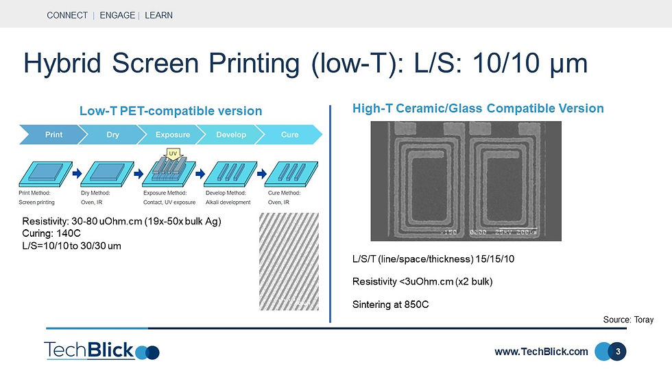
The approach is shown schematically below. A photo-patternable screen printable paste is developed, which can be directly photolithographically patterned without requiring an additional photoresist deposition and development step. The low-temperature PET-compatible version of this paste enables L/S as narrow as 10/10 µm. However, the achieved conductivity is not the highest (around 30-80 uOhm.cm when cured at 140C). The high-temperature version of course goes higher in conductivity, approaching x2bulk (3uOhm.cm) when sintered at 850C.
This solution is particularly suited to touch screen edge electrodes based on ITO on PET substrates since (a) it enables narrow edge electrodes (lower L/S) and (b) ITO film patterning requires photolithography in any case.
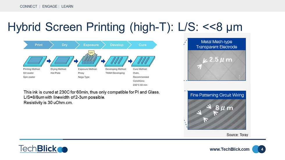
This approach can be finetuned to support even narrower L/S. In this example, you can see fine circuit wiring and metal mesh examples, reaching 8µm and 2.5µm linewidth, respectively. Note that at 2.5µm linewidth, this hybrid printing process approaches the best-in-class metal mesh linewidths. This technology still has some limitations though, namely, a high curing temperature of 230C, (which is not PET, PEN, PC compatible) and only a moderate paste resistivity.
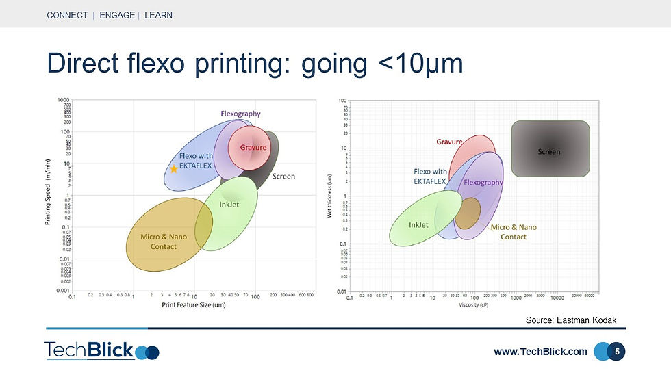
There are many reasons why one may want to print using a technique other than screen including higher print web-speeds, finer feature sizes, and lower print thicknesses. These two charts, developed by Eastman Kodak, offer an insightful map. The left chart shows that flexo, gravure, and inkjet are better suited in forming thinner lines using lower viscosity inks. The right chart shows that inkjet, flex, and various mico-nano contact printing processes enable features sizes in the sub-30µm territory.
Kodak has further advancement the art of high-speed flexographic printing of functional layers. In particular, their flexographic plates with flat top dots and high resolutions (achieved with well-designed non-Gaussian lasers) enables finer features. Here, on the left, an example of a flat top dot plate can be seen.
In the right, an example of fine line printing is demonstrated for an RF antenna application. Here, a thin catalytic layer is flexographically printed and then Cu plated to achieve high bulk-like copper conductivity, required for good antenna performance. The printed linewidth can be as narrow as 7.8µm, demonstrating the fine line printing capability of this process.

Below is an example of a gravure offset process developed by Komura Tech in Japan, directly printing continuous unbroken lines with sub-5um linewidth.
Note that it is an ‘offset’ process, and as we will see, most sub-5um printing techniques involve an ‘offset’ step. Here the inked gravure roll first transfers the paste onto a blank role, which then transfer it onto the substrate. One advantage of this approach is that the ink can be partially dried before reaching the substrate, thus preventing wetting-related issues which limit linewidth capability.
This technology enables fine metallization of circuits on flexible substrates. The lines are currently based on Ag NPs and are likely to be very thin (250-300nm).

Below is another example of ‘offset’ based printing, Shashin Kagaku in Japan, demonstrated S2S direct printing of thin (250nm) layers of Ag nanoparticle inks with linewidths as narrow as 1.5µm in complex patterns. The process can be on glass and PET (note: influences also the achieved sheet resistivity due to difference in allowed curing temperature).
An obvious target market is metal mesh TCFs and here they can demonstrate 0.2- 0.3 Ohm/sqr sheet resistance at 150C (PET compatible range).

Here is yet another example of ‘offset’ based printing developed by VTT (Finland). In this reverse offset process, the PDMS roller is first coated with the ink. The ink semi-dries on the roller, partially through absorption into the PDMS. This semi-dried state allows one to overcome wetting-related issues when inks are in liquid state. The inked PDMS roller is brought into contact with a Cliche, or relief plate, removing parts of the inks. The patterned semi-dried inks on the PDMS roller are then transferred onto the final substrate.
In this example VTT achieves 1µm direct printing of silver nanoparticle inks. The small-sized RO printer was used to print a metal mesh on PET with 1µm linewidths. The reported sheet resistivity is not very low (100Ohm/sqr), probably because the lines are very thin.
Note that ROP can enable minimum resolutions between 0.5-5µm, printed thickness lines around 20-1000nm, overlay accuracy <2um, and printing speeds of 50mm/s (3m/min).
In all the examples demonstrated thus far, a printed conductor (mainly Ag NP ink) is printed. However, this ultrafine line printing process can also print photoresist, enabling one to replace photolithography in some cases.

The final direct ultrafine line printing process I wish to highlight is by Asahi Kasei. Here, sub-1µm unbroken straight as well as shaped lines are demonstrated. For example, in the right image, one can see a continuous 300nm wide lines, as well as TFT patterns printed for 2000 ppi (pixel per inch) resolution [here, the entire TFT pixel pitch is 12.5um)
The exact process is not disclosed, but our guess is that it is a R2R reverse offset process. Here, as the case before, an ink system applies the ink onto a blanket roller. A roller mold containing the final pattern is brought into contact with the inked blanket roller, removing parts of the ink to form the pattern. Finally, the blanket roller transfers the pattern onto the final substrate.
A key technology step here is in the formation of the roller, which essentially enables R2R nanoimprinting. Here, no laser is deployed. Instead, an electron beam lithography (with multiple exposure lines) is used to create ultrafine features. In the case, the roller is first dip coated, exposed to EB, developed and backed. The accuracy of this process is shown in the middle pictures, demonstrating 1µm linewidths in 5µm pitches. Currently, the rollers is available in 250mm width and 100mm diameter size or smaller. Our guest is that the current web speed is 1m/min or slower.
Asahi Kasei is targeting TFT backplane metallization as well as transparent RFID antennas. Transparent RFIDs enable ones to print graphics on all parts of the package since they block no area. This narrow-line printing technique can also have security applications.

So far we covered direct printing (except for screen printing). Many ‘hybrid’ solutions are also developed to enable ultrafine line features. This example is by Panasonic, although many others such as O-Film developed similar technologies before. We select the Panasonic example because it is a technically sophisticated solution, achieving 2µm features on both sides of the PET film.
In this approach, fine grooves are first embossed into the film. The Ag NP inks are then used to fill in the groove (probably with a doctor blade). There are some core benefits here: (1) linewidth is set by embossing, which is free from wetting characteristics of a liquid or even semi-dried ink system; (2) conductive lines are embedded meaning that the surface is smooth; (3) high conductivity levels can be achieved even with printed inks without compromising linewidth or surface smoothness.
The final point is worth further consideration. In normal cases, to increase conductivity, wider and/or thicker lines are needed. Here, to increase conductivity, one can increase ‘depth’ of the groove (although this is also subject to various limitations).
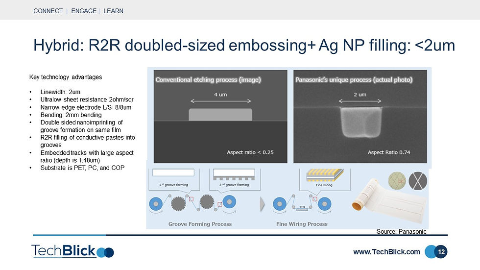
The slide below shows a variation of the previous concept. Here, the innovation is to first create a thin Ag NP seed layer (with doctor blading) within the embossed groove before Cu plating. This approach results in high conductivity as plated Cu, and not printed paste, is used. Consequently, it enable it efficient large area transparent heating applications.

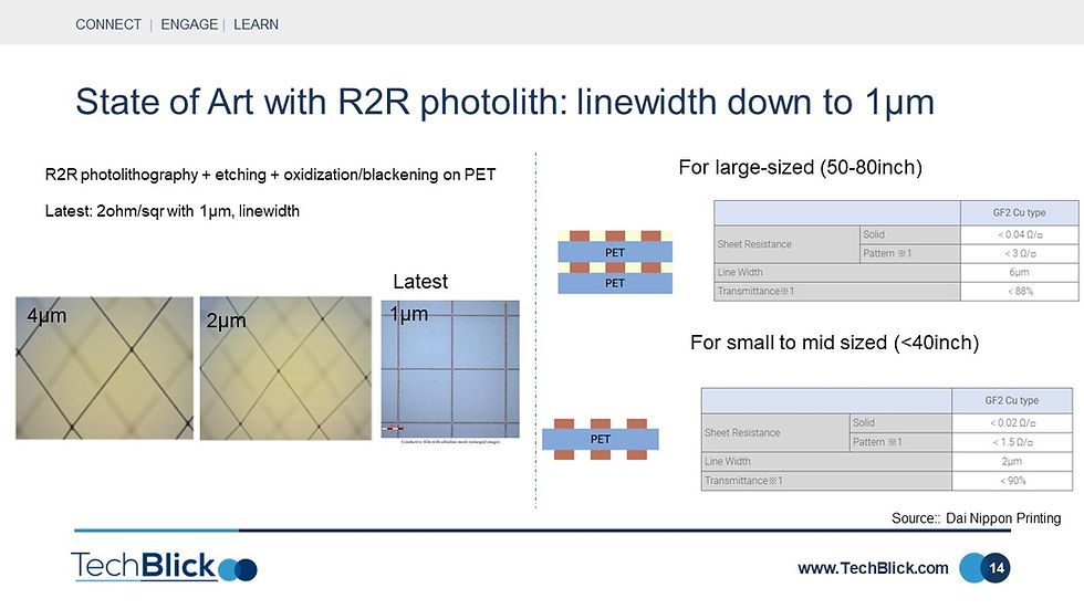
Just a reminder, that photolithography, including R2R photolith, can also create ultra fine features including metal mesh. I include an example here by DNP (Dai Nippon Printing) which represents the state-of-the-art. In previous generations, 2um lines could be achieved for mid sized double-sided metal mesh films with 1.5 Ohm/sqr sheet resistance. The latest results are metal mesh films with 1um linewidth and 2ohm/sqr based on etched copper can be achieved. This is included here to showcase the performance level of the alternative non-printed technology.
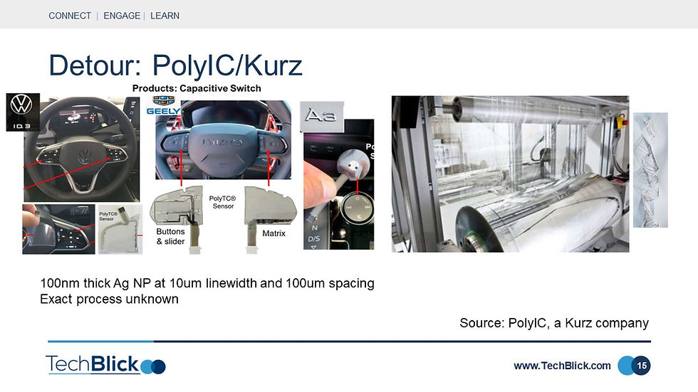
Finally, on this theme, I would also like to showcase the metal mesh films by PolyIC, Kurz. The metal mesh films have 10um linewidth and 100um spacing with ultrathin (100nm) layers of printed Ag NP. I include these last because I do not know the exact printing technique.
Note that these capacitive touch films are already commercialised in automotive application, replacing mechanical with capacitive switches. In addition to metal mesh properties, a key innovation here is the so-called Functional Foil Bonding, which enables these metal mesh films to be integrated on the back of shaped plastic parts together with decoration layers.
Innovations Festival: Printed, Hybrid, 3D, InMold, Textile Electronics
24 June 2022 | 14:00 - 19:00 CET | Virtual Event Platform
Asada Mesh will be having a virtual booth at the Innovation Festival. Visit Asada Mesh virtual booth


Comentários