


R2R grown GaN LEDs and perhaps even GaN/AlGaN HEMT transistors on metal foils instead of expensive small-area sapphire substrates? This could be a breakthrough technology, bringing the robust and efficient inorganic LED technology to large-areas. In microLED displays, it could mean monolithic integration, leading to mobile-sized and large displays manufactured without a wafer-to-substrate transfer step.
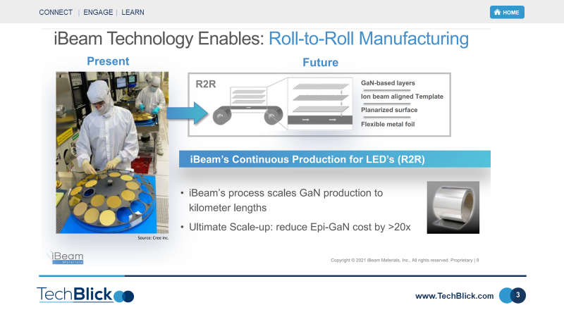
As shown below, iBeam Materials is developing such technology. It first planarizes a rough metal foil and then uses an ion beam to form a nm-thick layer with aligned grains. This 'template' then acts as the growth substrate in lieu of, say, a sapphire wafer.
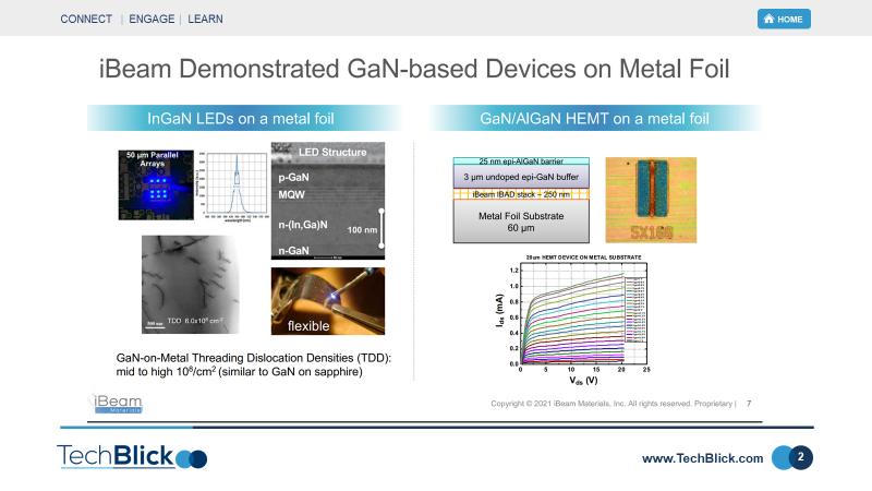
As seen below, this technology has already been used to demonstrate a functional GaN LED as well as a GaN/AlGaN HEMT. In July 2021 (when the results were presented at TechBlick) the PL was upto 70% of normal LEDs. However, a direct comparison is not yet fair as the standard approach benefits from decades and decades of accumulated know-how and production expertise.
Currently, the LEDs are still not done in a R2R fashion, although the 'template' can be R2R manufactured on 20"-wide substrate. The next step of development will involve demonstrating a R2R MOCVD GaN growth. The R2R production of the template is not the bottleneck, but the growth of a thick (5um or so) GaN LED
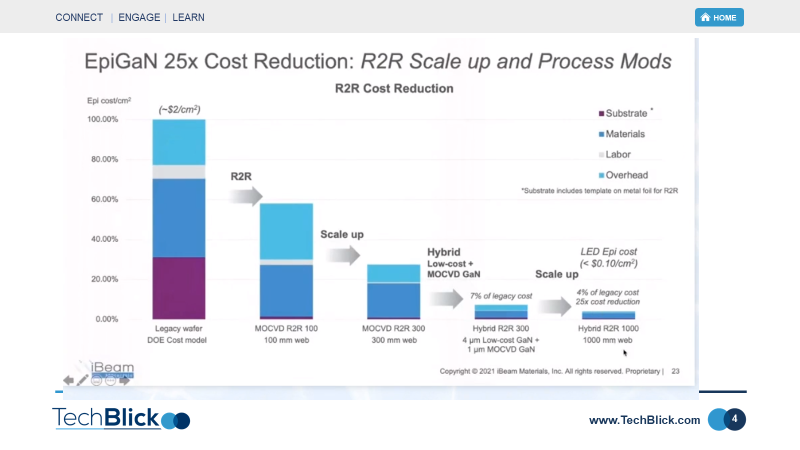
Finally, Vladimir Matias argues that this technology has the potential to lower cost of production by a factor x25. A detailed cost analysis is shown below, demonstrating the technical milestones which need to be achieved to enable this cost roadmap.
To learn more about this talk and about microLED join TechBlick first-ever specialist event on microLEDs:
www.TechBlick.com/microLEDs
@klauz kunze


Comments