Marja Vilkman from VTT will present the latest on the theme tomorrow at TechBlick's event on Perovskite, Organic, CIGS and Tandem Photovoltaics - check out the agenda now www.TechBlick.com
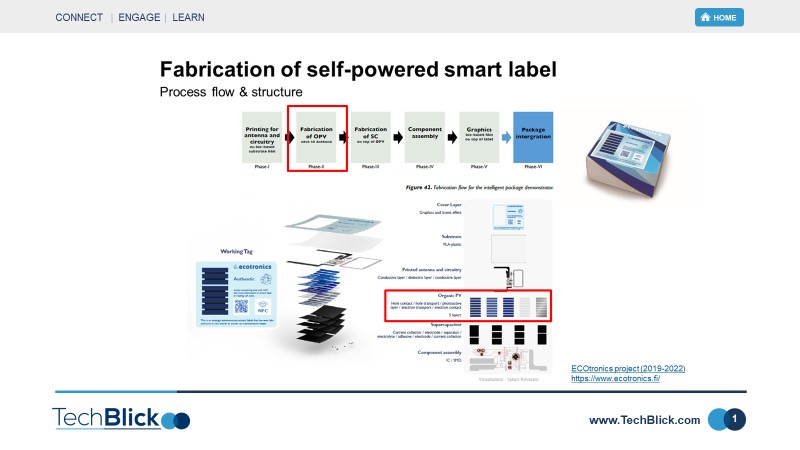
First slide depicts the structure of the smart label and the associated package design optimized for the best performance, functionality, and appearance.
The labels were fabricated according to process flow described in the upper image. Biobased PLA and commercial fossil-PET (as a reference) films were chosen as base substrates for the labels. Silver and dielectric were screen printed for the antenna and circuitry. Organic photovoltaics (OPV) was printed next to the antenna, the supercapacitor on top of OPV and, surface mount devices (SMD) were assembled with isotropic conductive adhesive. The printed graphics film on biobased substrate covered the label. The graphics film was designed to provide the information for the user and comprised embossed feature for authentication.
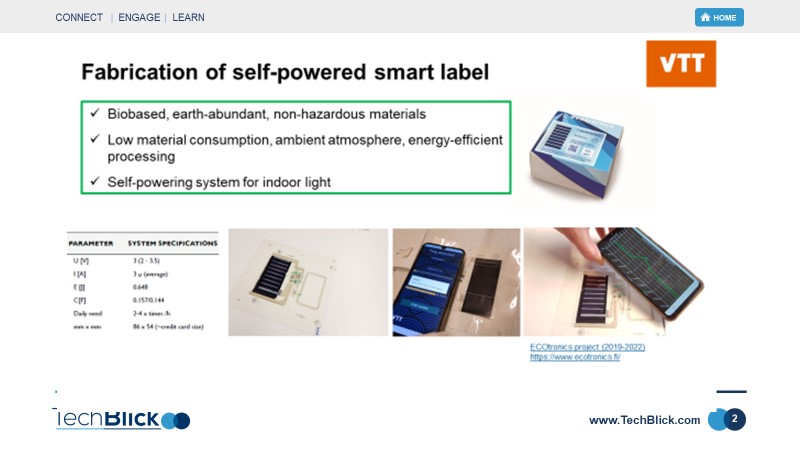
Second slide presents the use of energy autonomous smart label for the temperature monitoring of the secondary packaging. Intelligent packaging is a relatively new application domain, and it has specific expectations as the smart label comprising electronics would need to be cost-efficient, recyclable, and lightweight. Aim of the product design was to identify the opportunities of the intelligent product packaging using new materials and production processes to improve material and production efficiency and, product properties e.g., climate impacts, resource savings, functionalities, and usability.
Join us tomorrow to learn more www.TechBlick.com


Comments