Printed electronics and power electronics? There is a direct link via die attach materials. Indeed, this is a success story but as with many other such stories in printed electronics, it gets called something else once it reaches the market. So what is this story?
Many die attach systems in power electronics (IGBT Mosfets, SiC, GaN, LEDs, etc) continue to use solder. Thanks to wide band semiconductors *WBS), the trend is towards ever higher areal power densities which translates into higher junction temperature. Indeed this shift to WBS means that the semiconductor is no longer the limiting factor, but the packaging materials.
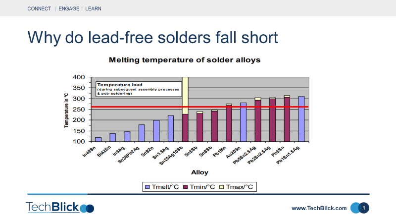
One such material that falls short is lead-free solder. At operating temperatures like 175C (target is 200C and beyond), the max temperature of the solder should be 265C if the homologous temperature is to be 50% or less. The first slide below shows that lead-free solders do not have a high enough melting temperature. The common SAC solder falls clearly short. AuSn or SnAgSb might be options, but even they are forced to operate near their limit.
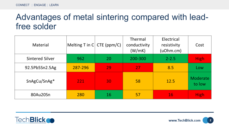
To solve this shortcoming, sintered metal die attach materials (Ag and Cu) offer a good alternative. The table in slide 2 table shows that sintered Ag (also Cu) has a bulk-like melting temperature, enabling very high operating/junction temperatures. The thermal conductivity – depending on the sintering- can be very high, even much higher than AuSn.
The technology is already commercial for many years in places like Tesla cars (Ag sintered die attach on SiC power electronics). It is a market that will grow as electrification of the vehicles continue apace. It will also be boosted further as GaN power amplifiers gain a foothold in 5G communication infrastructure.
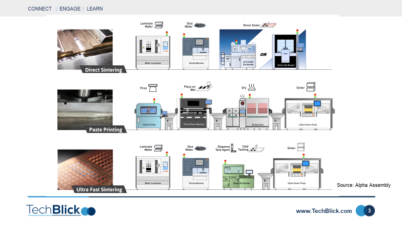
The sintered metal can be applied in different ways. In the printed case, the die attach paste (containing Ag or Cu particles) can be stencil printed or screen printed or dispensed. For ‘pressured’ versions, the most common approach is to screen print the paste, pre-dry it, position the die and pre-heat the substrate, and sinter under pressure. The target is to form a strong adhesion and to form a bondline free of voids and as much solid-like as possible. This is why sometimes external pressure is applied to squeeze out all the voids and form a compact solid-like bondline. In another technique a dry film can laminated onto a wafer. The dies are therefore picked with the die attach already applied. Alternatively, one can using a dry film
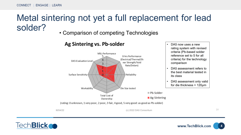
This technology has come a long way. There are now many pressure-less versions with also rapid sintering. Both nano and micorn sized particles are used. The technology also now gives good bond strength even on non-matching surfaces (e.g., applying Ag die attach on a Cu surface). Nonetheless, it is still not a full replacement for lead solder
The chart in the final slide is an excellent study recently published by a DA% Consortium offering a real benchmarking based on tested results. Thus, the technology wins when lead can not be used, the costs can be tolerated, and lead-free solder falls short. However, it still has room for improvement to match the best in class of lead-based solder
Join www.TechBlick.com to learn more






Comentarios