MicroLEDs, printed electronics and laser printing?
- khashayar Ghaffarzadeh

- Sep 29, 2022
- 2 min read
Holst has developed and advanced the so-called LIFT technology to enable even the laser transfer or laser printing of microcomponents such as microLEDs with high 1-um precision.
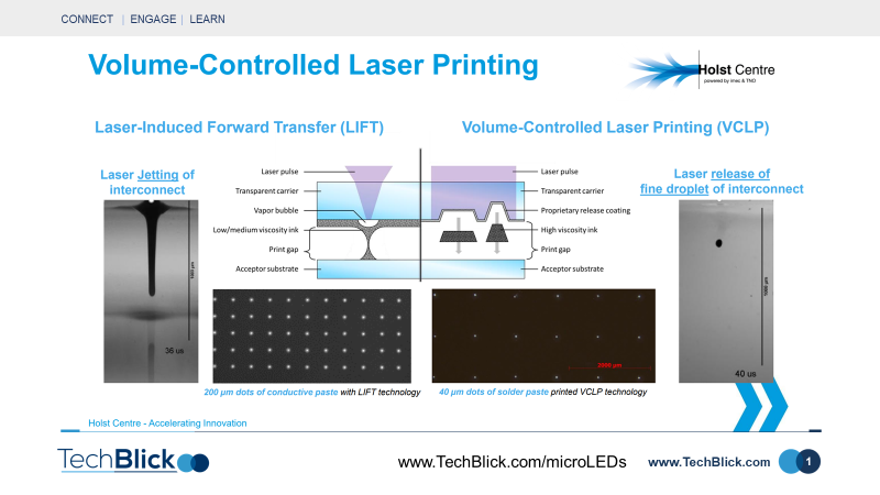
In the first slide you can see a comparison of the classical Laser Induced Forward Transfer (LIFT) vs the technique developed at Holst which is Volume-Controlled Laser Printing (VCLP).
In LIFT, the laser illumination causes a jetting of low to medium viscosity inks onto the acceptor or target substrate. This is not a young technology and some consider it the digitization of screen printing. In the example here you can see 200um dots of conductive paste printed with the LIFT process.
The VCLP is different. Here, the laser releases fine droplets onto the target/acceptor substrate. Given the volume control, better resolution is accessible. The example herein shows 40um dots of highly viscous solder paste printed using VCLP technology. Note that here the high-throughput deposition of ultrafine interconnects, such as conductive adhesives and solder pastes, is from a structured carrier plate covered with a proprietary permanent release coating
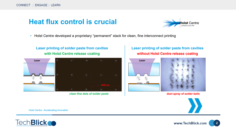
An important feature of the VCLP technique is the control of heat flux. Without this the laser printing can result in blurred or poor definition. To manage the heat flux, Holst has developed a proprietary “permanent” stack for clean, fine interconnect printing. In the second slide, you can see the positive impact of this layer in achieving well defined high resolution laser printing
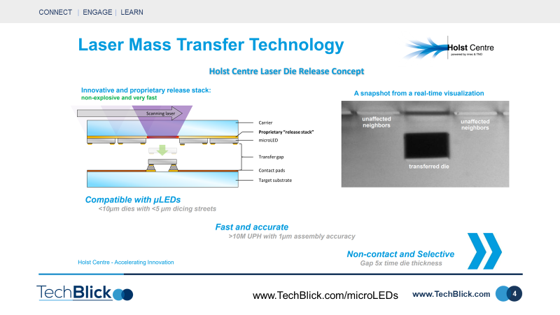
What is amazing is that not only inks and pastes (also adhesive and solders) can be printed, but also microcomponents such as microLED dies. In the schematic in slide 3, you can see the concepts. Here, the microLEDs sit on the proprietary “permanent” stack and are then laser released across the print gap onto the acceptor/target substrate. The dies can be <10um with a <5um dicing street. This technique can reach >10M UPH (units per hour) with 1um assembly accuracy
The final slide shows examples of mini as well as microLED transferred using this technique. The mini LEads are 125x125x80 um3 and the microLEDs are 60x60x10 um3
This are incredible results and points towards a new high throughput laser printing technique able to print finelines of inks as well as highly viscous pastes, and mini and micro components
To learn more you can either join us onsite at the High Tech Campus where the Holst Centre is also located on 12-13 OCT 2022 and join our microLED event online on 30NOV-1Dec where this technology will be presented
https://www.techblick.com/electronicsreshaped
www.TechBlick.com/microLEDs


Comments