


microLED display technology requires massive parallel transfer technology. This is a complex technology as it is and will grow even more complex as displays with smaller dies and high PPIs are considered. This has been one of the frontiers of development in the uLED industry.
Many parallel transfer approaches have been proposed. Most are based on a type of stamp which picks up the microLED dies from the growth substrate and transfers them onto the target substrates, placing them at the right spot.
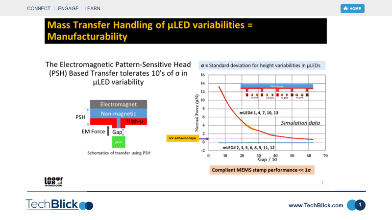
A critical challenge is how to overcome inevitable height and dimensional variations of uLEDs using standard elastomer-based microLED technology, which, if not managed properly, can adversely impact that all-important figure-of-merit: yield!
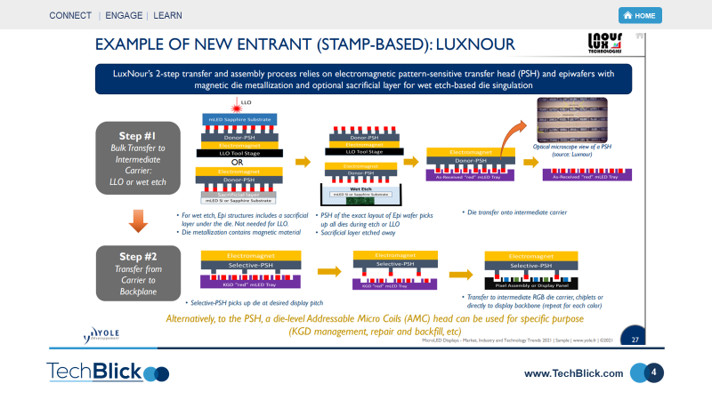
LuxNour Technologies Inc. is proposing a novel approach based on electromagnetic stamps which can - as shown in slide 1- tolerate tens of σ in uLED variation! This increases yield and eases the pressure on exact control of the microLED dimensions during the growth. Join the specialist TechBlick conference on microLEDs on 30-Nov and 1-Dec to learn morewww.TechBlick.com/microLEDs
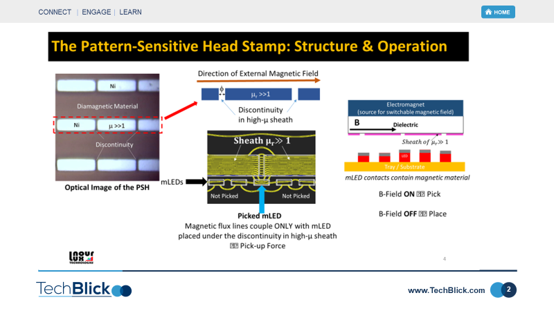
Makarem Hussein in slide one shows the structure of such an electromagnetic head, containing a bulk electromagnetic at the back, a non-magnetic dielectric element in between, and a pattern of high permeability materials (e.g., Ni) and openings. The high permeability areas shield the bulk magnetic, preventing its flux from protruding out. In contrast, the openings represent discontinuities in the shield, allowing the EM force to penetrate out. Slide 2 shows a close up of the structure as well as the resultant magnetic flux
In this approach, the microLEDs will also require a layer of metallization with a ferroelectric material. As shown in slide 2, when the magnetic field is on, the microLEDs - regardless of height variations - are picked up by EM force at the location of openings/discontinuities. When the field is off, the dies are released (or placed).
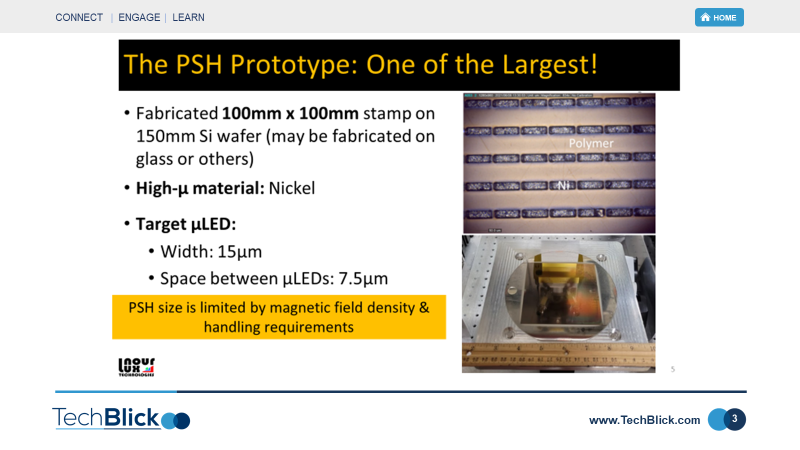
Slide 3 shows an example of a100mx100mm stamp on a 150mm Si wafer. Here, the high-permeability material is nickel. This stamp can handle 15um microLED dies with spacing of just 7.5um.
This is a very interesting technology with excellent potential. Of course, there is significant know-how and expertise and technology in EM stamp/head development (see patent: ). Furthermore, the microLED wafer manufacturers must adopt their metallization step to depost a ferrous material.
Makarem Hussein will join speakers from Samsung, Sharp, AUO, ST, Coherent and many others to discuss the present and future of microLED technology on 30 NOV - 2 Dec - see agenda here www.TechBlick.com/microLEDs


Comments