


Innovations Tour in Additive Electronics: From Analog to Digital Printing | Fineline, high viscosity, and 3D
- khasha8
- 4 days ago
- 15 min read
In this article, we highlight a number of printing process innovations that are advancing the state of the art in printed and additive electronics and are addressing critical existing limitations to open new opportunities.
Here, we will go on a quick tour from analog screen printing to digital printing to ink-less laser printing. In this journey, we will make many short stops covering screen printing, capillary printing, inkjet printing, EHD printing, micro-dispensing, LIFT printing, dry printing and beyond.
Wit over 25 images, tables, charts as well as 13 videos, we cover the following points
Screen printing: State of the art ultrafine line printing
High production speed in screen printed metallisation
Rotary screen printing for PV metallisation
Alternative PV metallisation methods (1): Capillary printing
Digital printed electronics/additive electronics
Can we scale up inkjet printing in functional printing?
How to digitally print high viscosity pastes?
Digital multi-material laser printing of high viscosity pastes in printed electronics and electronics manufacturing
High viscosity digital printing AND ultra fine resolution well beyond inkjet or LIFT
Digitally printing higher viscosity levels at ultrafine resolution without e-field?
High Pressure Capillary Printing - high resolution, high aspect ratio and high viscosity printing without e-fields, satellites or splashing?
Printed Electronics / Additive Electronics without inks?
SSAIL Process: Additive laser-induced metallisation of "diverse" surfaces
Dry (Ink Free) multi-material direct laser printing
To learn more about the wonderful world of Additive and 3D Electronics, join us and 550 others from around the world at the Future of Electronics RESHAPED conference and exhibition in Boston on 11 and 12 June 2025.
This is the largest and the most important event in the US dedicated to Additive and 3D Electronics, bringing together over 550 participants, 70 talks, and over 75 exhibitors.
Explore here https://www.techblick.com/electronicsreshapedusa
Major Early Bird Ends on 25 April. Go HERE to receive a coupon offering you 200 USD additional discount on top of early bird rates.

Screen printing: State of the art ultrafine line printing
First let us start with one of the largest applications of printed electronics: photovoltaic metallisation. In fact, this application is so large that according to projections this market alone will end up requiring amounts of silver in excess of 100% of the current worldwide silver supply soon, meaning that silver shortage will constrain growth if technological changes do not address the issues.
In PV metallisation screen printing has been completely dominant despite many attempts to introduce alternatives. Here, screen printing is the state of the art, pushing the boundaries of what is considered possible every year.
The chart below shows the research level progress in ultrafine screen printing in photovoltaic metallisation. It shows that the state-of-the-art linewidth at research level went down from 80-10 µm in 2008 to 17µm or so now. This is an incredible rate of progress and learning.

But the progress in fineline screen printing is not limited to just research. The industry has actually followed too given the strong need to print ever narrower lines without efficiency loss to reduce silver consumption per cell or watt.
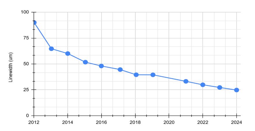
This is shown in the chart below which TechBlick has compiled from years of ITRPV roadmaps. The chart shows linewidth of screen printed metallisation as a function of year, demonstrating that the linewidth in mass production has gone from some 90 µm or so in 2012 to now 25 µm. This is just an incredible advancement of the art of screen printed electronics. This achievement is the result of real team effort between printers, screen and mesh makers, paster makers and equipment manufacturers.
Below you can see an example from Fraunhofer ISE showing how they managed to improve the topography of the printed lines, making them ever narrower with an aspect ratio of 1. This progress is the result of years of hand-in-hand effort in paste optimisation (rheology, particle size, wall slip, etc), mesh technology (e.g., towards ultrafine 520-11 stainless ones), and emulsion-over-mesh (EOM) technology (e.g., laser opening of EOMs with sub 20 µm openings and ultra long life (80k-100k) print runs in PI), etc

High Production Speed in Screen Printed Metallisation
But in this business of PV metallisation, it is not just the linewidths that are impressive, the production speeds and throughputs are also very impressive.
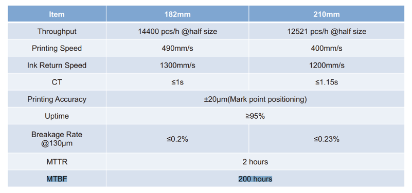
As an example, below you can see a printer by Suzhou Maxwell Technologies Co., Ltd. in action. This is a new half-cell TOPCon printer. The parameters are reported in the table below, showing that this equipment can achieve 14400 pieces per hour at half cell at printing speeds of 490 mm/s and a cycle time (CT) of >1s with minimal breakage. This is impressive!
Below you can also see a full turn-key automatic line for full-size wafers. This data is also from Suzhou Maxwell Technologies Co and was presented at TechBlick in 2023, so is already 2 years old and still impressive!

Rotary Screen Printing
In production everyone uses flatbed screen printing. But can one also utilise rotary screen printing whilst meeting the linewidth and aspect ratio requirements? Here you can see an example from Fraunhofer ISE again showing a rotary screen printing line which can achieve in a single printing line some 8000 SHJ wafers per hour with a cycle time of just 0.45s at a linewidth of 50um or so. This is impressive for a demonstrator full system machine although it is not yet commercial. In general, given the exacting linewidth requirements and the current status of flatbed screen printing systems, rotary screen printing will not find it easy to go from pilot to production in this application.
Alternative metallisation methods (1): Parallel dispensing
Many alternative processes have long sought to replace or at least dent the dominance of screen printing. Here I want to highlight some interesting approaches being developed by the community.
First example is from Highline Technology which uses parallel dispensing or homogenous extrusion of metallisation pastes through parallel nozzles. The image below shows the paste being extruded outside the nozzle, and the video below shows the printing process at a pilot equipment.
This is an interesting process because it is non contact and can achieve finger widths down to 20 µm with good print speeds exceeding 500 mm per second.
Furthermore, this printing process can yield nice printed lines with excellent aspect ratios. This is shown below. The left images show printed aluminium traces whereas the right one shows silver lines with a linewidth of 17 µm and a good aspect ratio.

Alternative PV metallisation methods (1): Capillary printing
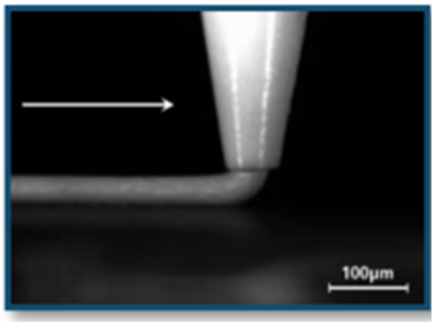
Another innovative approach is using capillary printing under pressure. We will come to capillary printing again in another context later in this article. Here the capillary, made out of glass with a narrow 20 µm opening, is brought close to the surface and atmospheric pressure (10 mbar to 11 bar) is applied, pushing the paste out, thus printing at speeds up to 500 mm/s. The process is schematically shown below.
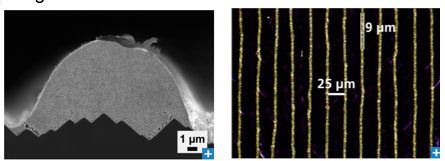
You can see also some print profiles, showing the capability to achieve ultra narrow line with good aspect ratio. Here Ag NPs inks are used since larger particles could clog the glass capillary.
When applied to a single heterojunction cells the process could achieve 12 µm lines with 6.4 µm height, resulting in a good SHJ efficiency of 22.96%. Critically, this process could lead to 60% less silver consumption.
These are impressive results. However, this is relatively early stage and much work needs to be done on parallelisation and on achieving stable print runs.

Digital printed electronics/additive electronics
Now lets switch from analog to inkjet and DIGITAL printing. The most traditional digital printing method in printed electronics and additive electronics is inkjet printing (IJP). In fact, IJP sets the reference point, and many innovations and developments covered in the rest of this article seek to address the shortcomings of IJP, such as IJP's inability to handle high viscously pastes or its limited print resolution.
Can we scale up inkjet printing in functional printing?
One common question has always been whether one can really scale the size of inkjet printers when it comes to functional printing. As seen in the image below, the answer is YES!
Below one can see a huge inkjet printer - by Kateeva - able to print on Gen 6.5 glass (925x1500mm2) glass. To appreciate the size of the system, it is instructive to see the human next to the machine in the image! This is a commercial system used in production of multilayer encapsulation layers in OLED displays where the organic layer in the barrier is inkjet printed. It is thus area printing and not pixel printing.

The video below also shows how the printing actually works, showing the movement of the print heads as well as that of the glass floating on gas. This is an incredible feat of engineering in inkjet printing millions and millions of droplets over huge areas in a production setting.
How to digitally print high viscosity pastes
A major shortcoming of IJP has always been its inability to print high viscosity materials. There are many approaches to enabling digital printing of high viscosity materials like screen printable pastes, adhesives, solder, and many other materials.
An interesting approach has been taken by Quantica. An example of their print system is shown below. They essentially build a powerful actuation system within the print head able to push out even high viscosity materials.
The parameters are shown below. The print head can handle pastes with viscosity levels up to 240 centipoise that have a high loadings (>75 wt%) and even large particulate fillers (5um or so). Thus this print head can open up jetting to all manners of higher viscosity materials including screen printable pastes.


There are however a couple of challenges that still hinder rapid and widespread adoption in printed electronics. The first is the need to have custom-made pastes necessitating a close collaboration with ink/paste makers who are willing to make such custom formulations. This is because the print head operates at 80C or so. This would mean that most standard screen printing pastes would already begin to dry in the print head and within the circulation system, limiting print runs and stability. This can be addressed with special paste formulation, however.
The second current challenge is the limited number of nozzles per print heads. This is the consequence of the fact that the actuation mechanism takes up real estate in the print head design, inevitably limiting the number of possible nozzles.
Digital multi-material LASER printing of high viscosity pastes in printed electronics and electronics manufacturing?
Another interesting process enabling digital printing of high viscosity pastes is the LIFT (Laser Induced Forward Transfer) process.
The operation principle is explained nice in the below video by Coatema. The process works by first coating the paste on a transfer film. A laser then run across the transfer film causing the coated material to be released at points which are laser illuminated. The released materials then land onto the target substrate. Thus the process can digitally with the help of a laser essentially print the material! It can even be done R2R!
Interestingly - as shown in the table below - this method can print materials with a wide range of viscosities, ranging from 500 to over 300 000 centipoise. Indeed, in the table you can see that LIFT can print carbon pastes, ceramic pastes, metal pastes, solder, silicon, and even epoxy!
The print resolution can also be as low as 40um, thus being comparable to the very best-in-class advanced screen printers found at most contract manufacturers in the printed electronics and electronics manufacturing operations.

Below you can see the solder printing in operation by an io-Tech LIFT printer machine. It can print T6 solder at 120 um and T9 at 45um, operating at 5 million drops per hour (equivalent to some 13888 drops per sec). This is thus a high speed and high resolution process able to handle a wide range of viscosity levels.
What is unique is that in the same print run - by controlling the laser profile - one can print two different profiles. See the example below. These were done in the same print run! This opens up some nice possibilities.
Interestingly this process also be made R2R. This is explained by Coatema, which is developed such a system, capable of printing on 180mm wide substrate at print speeds of 2-10 m per min and resolutions of up to 600 dpi.
Key innovations here will also include ink recycling as well as rapid laser drying, which is more digital and energy efficient than general overn curing (but less flexible and more material specific). This will open up the way for digital and roll-to-roll mass production on flexible substrate. This is important because previous attempts with inkjet printing were not always successful due to limited material menu and process instability
Here it is important to mention that ink recycling is crucial. This is because only a small fraction of the paste coated on the transfer film will be printed. Thus - without recycling - the process will be extremely wasteful with a poor material utilisation, which will increase costs, potentially rendering it unviable. Thus this is an important process innovation.
High viscosity digital printing and ultra fine resolution well beyond inkjet or LIFT?
Thus far we have seen that it is possible to digitally print high viscosity materials. But both mentioned processes have low to moderate resolutions. We will now showcase a range of printing techniques that enable ultra high resolution printing of even high viscosity materials.
The first process is EHD (Electrohydrodynamic) Printing. Here, an electric field build into the print head is used to pull out the ink and particles. Thus it is not a classic push process as in inkjet printing. This means that EHD printing can handle much higher viscosity levels and can have narrower nozzles with more focused jets leading to higher resolutions. The schematic below by Scrona shows the design of a multi-nozzle print head showing that each nozzle could be ca 200um wide with its own well-controlled e-field.

This process can print with resolutions of 500nm or handle materials with viscosity levels over 10 000 cP. The video below - also by Scrona shown at a TechBlick event - shows the printing of quantum dots (QDs) with a multi-nozzle print head (I think this is a 128 nozzle printer!)
A key innovation here is how to scale to multi-nozzle printing. Scrona has developed its own MEMS technology for this together with custom made drive electronics, ensuring small sized multinozzle printer heads with little nozzle-to-nozzle electric field interference
process can also handle high viscoisty materials. As shown below, the print head may need to be adjusted, for example, by having wider nozzles. This way it can even print adhesives as shown in the video below (both schematic and video are from Scrona)

Can we digitally print higher viscosity levels at ultrafine resolution without e-field?
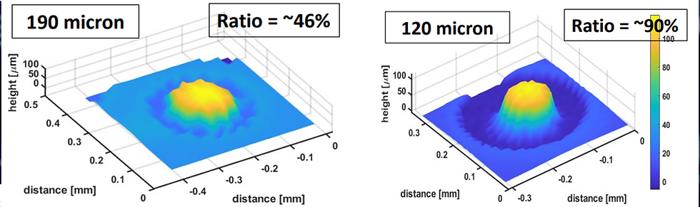
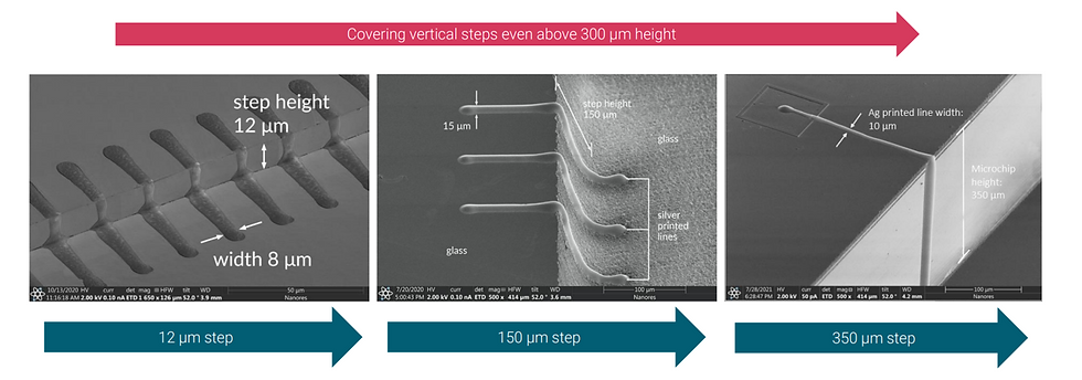
Micro-dispensing offers such a capability. This process - developed by XTPL - is shown in the video below. Here it can be seen that it can not only print ultrafine lines but also do so over 2.5D and 3D surfaces with steep steps, demonstrating the strengths of this process.
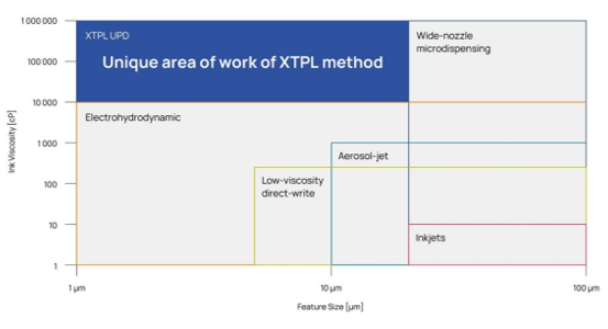
The chart below shows the market positioning of this process, indicating that it can also go where others can not, namely ultra high viscosity (10 000 to 1 000 000 cP) with a few micrometre resolution, enabling the printing of dense, high viscosity materials at ultrafine resolutions. Indeed the pictures below also demonstrate this, showing printed structure over 3D (over steep steps) at a few micron linewidth resolutions.
One question about this process has long been about print speed and productivity since here the print head hovers very close to the substrate often covering only a small area. However, as can be shown below the process is able to print fast at speeds of 8.3 dots per second. This indicates that the process can be industrialised with multiple parallel heads printing at high speeds.
High Pressure Capillary Printing - High Resolution, High Aspect Ratio and High Viscosity Printing Without e-Fields, Satellites or Splashing?
Another interesting process is the High Pressure Capillary Printing (HPCaP). Here the ink leaves under pressure a resonating pipette with a narrow opening which is vibrating very close to the surface - similar to an AFM system. As shown below, the technology can achieve sub-micron printing resolution and can handle high viscosity pastes up to 100 00 cPa. The technology does not use e-field and causes no satellite or splashing since print head is very close to the surface

In the image below you can see an example of a printed line, showing that it can print narrow linewidths as well as narrow pitches. The narrow pitch printing is important, demonstrating control of the print head and high control of the printed material without splashing or satellites

You can see below the printing process in action. Here a micro bump is being printed. This is a unique ability because in a single print run the process can print the entire micro bumps with high macro-scale height. This ability to reach macro-scale heights with micron-scale linewidths/diameters is unique amongst most printing processes. The process is rather slow however it still offers some unique value propositions even in this application. In R&D settings, it is much quicker to print micro-bumps and similar structures than go through a complex photolith process. In repair this process is also be unique especially if high aspect ratio printing is involved which most other printing processes can not handle.
Printed Electronics / Additive Electronics Without Inks?
Additive electronics is somewhat broader than printed electronics in that it includes techniques which are ink-free. Here we want to showcase two innovative laser-based and ink-free additive electronics processes: SSAIL and the NanoPrintek Process. They offer additive (or semi additive) way of manufacturing electronics
SSAIL Process: Additive laser-induced metallisation of "diverse" surfaces
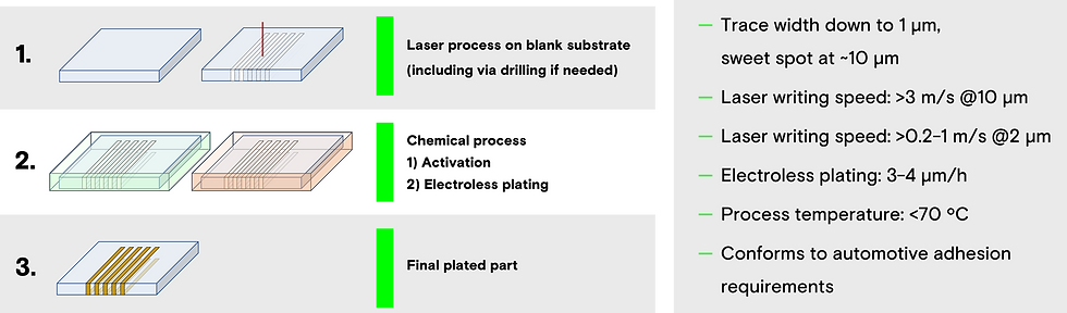
SSAIL stands for selective surface activation induced by laser! This is a unique process - developed by Akoneer in the laser hotspot of Europe, Lithuania - enabling metallisation of diverse surfaces. This is important because traditional LDS (laser direct structuring) is limited to a narrow set of specially prepared materials containing conductive particulates near the surface which can be exposed by laser illumination. In SSAIL however, the process is not limited to such substrate and can be applied to glass, FR4, ceramics, and a range of materials.
The process is shown below. Here, the laser is applied onto the blank surface to create a pattern. A chemical process is then used to active the surface of the laser exposed areas. Finally, those activated areas are electroless plated to form the final part.
The process parameters are also shown below. The traces can be typically around 10um (down to 1um also possible), high laser write speeds at 3m/s @10 um, rapid electroless plating, mild process temperature, etc.
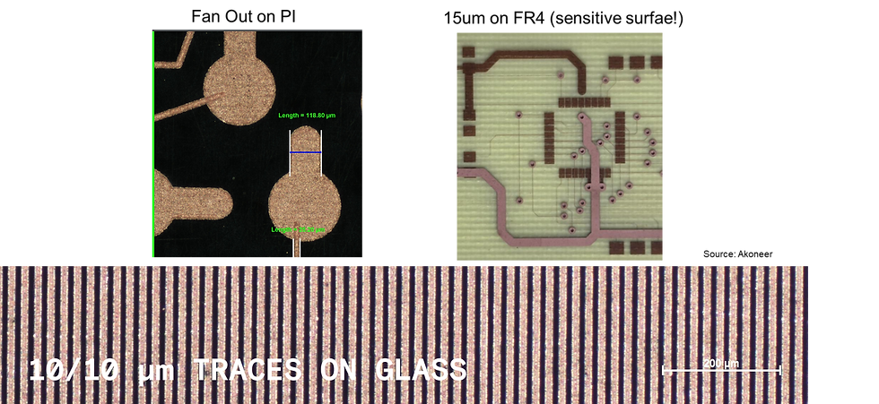
Below you can see three selected examples. All are made by Akoneer.
1) a fan-out Cu circuit on PI substrate with fine features,
2 ) 15um traces on a standard FR4 substrates, which is a sensitive substrates and demonstrate viability for PCB manufacturing,
3) 10um/10um Cu lines on glass
These applications show applicability to a wide range of substrates. They also demonstrate fineline capability. All these via an additive process with properties of electroless plated copper (vs those of conductive inks)
Dry (Ink Free) Multi-Material Direct Laser Printing
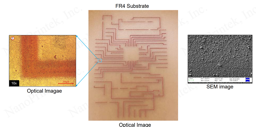
The final process we wish to highlight in this article is a novel dry ink-free multi-material printing process. The process is developed by NanoPrintek. It is shown below.
A solid target is inserted into the machine. The laser then ablates the material, forming nano particles which are then directed onto the substrate via nozzles. A sintering laser sitting below the print head then sinters the material.
The process does not involve inks and offers a high diversity of material options. The sintering and print steps happen at the same time. It is disruptive in the sense that it takes the ink our of the additive electronics / printed electronics process.
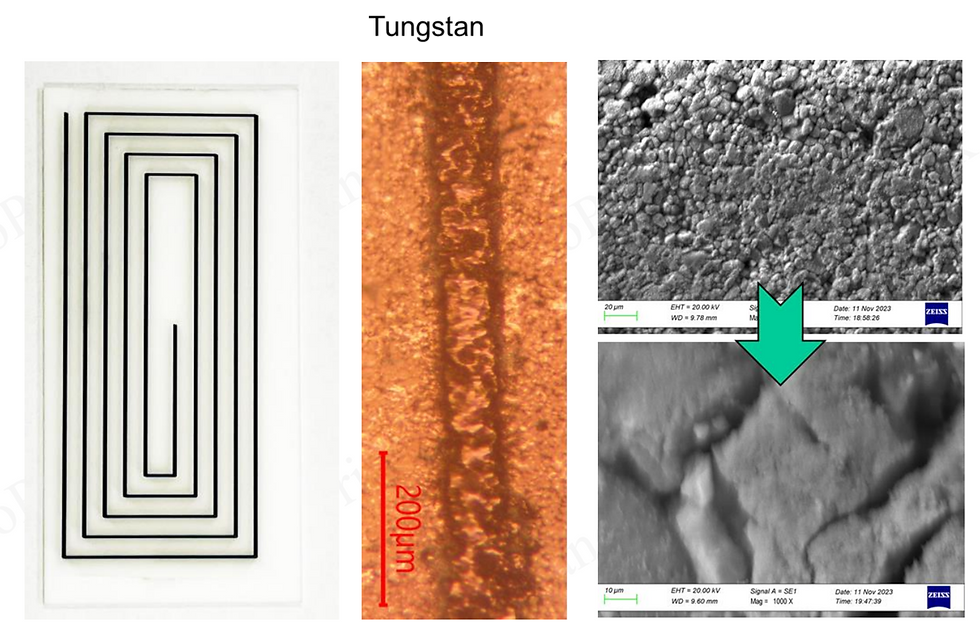
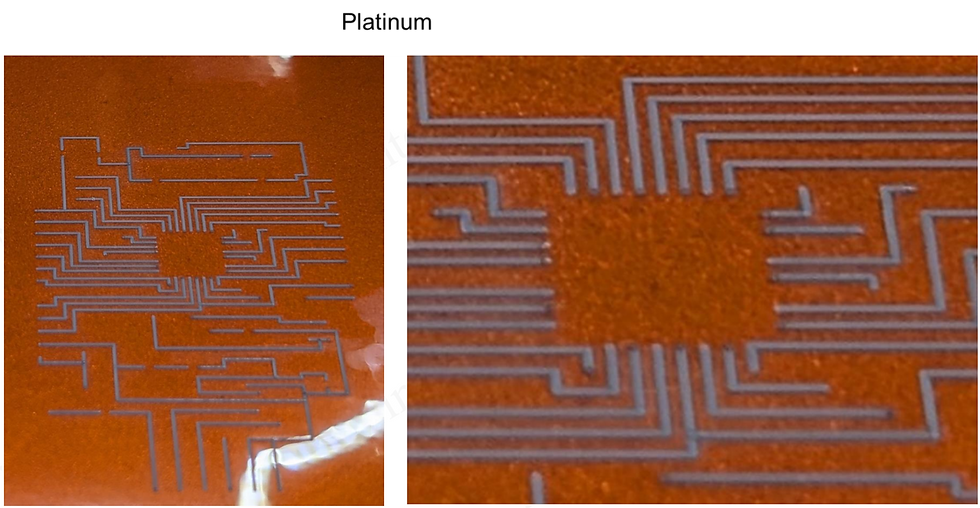
Below you can see various examples including
1) printing Cu on FR4 substrates
2) printing tungsten which is very hard to print via ink format
3) printing platinum which is very hard to print via ink format
The smallest nozzle is currently 100um but other nozzles are available too (150, 200, 300 and 350, 400um). In the near future, it is hoped that with aerodynamic focusing 20um effective nozzles and thus printed linewidths can be achieved. These are single aperture nozzle at the moment, but work is ongoing on multi nozzle system. Here the particle generated can be cranked up and the generated particles distributed through the multiple nozzle systems.
The system can achieve (as limited by nozzle diameter currently) 100um linewidth. It prints layer by layer. The printed layers are typically 200nm so to print thicker lines multiple print runs are required. This can be a limitation in many application where a relatively high current carrying capability is required thus thick paste printing will still make sense.
The work space is around 8inch by 8inch today.
The achieved conductivity today - without any sintering optimisation - is around one order magnitude below bulk. With optimisation of sintering, it is expected to approach bulk since pure metals are being printed.
Note that the sintering laser is below the print nozzle which means that sintering occurs at the same time as the print. The print speeds are up to 20mm per second. It is thus to be compared with other digital processes in productivity and not with the likes of screen printing which are much faster in printing in the same pattern on an industrial scale.
To learn more about the wonderful world of Additive and 3D Electronics, join us and 550 others from around the world at the Future of Electronics RESHAPED conference and exhibition in Boston on 11 and 12 June 2025.
This is the largest and the most important event in the US dedicated to Additive and 3D Electronics, bringing together over 550 participants, 70 talks, and over 75 exhibitors.
Explore here https://www.techblick.com/electronicsreshapedusa
Major Early Bird Ends on 25 April. Go HERE to receive a coupon offering you 200 USD additional discount on top of early bird rates.
Komentāri