


Indium Bump Interconnect (IBI) Flip Chip Bonding | finetech GmbH
- khashayar Ghaffarzadeh
- Feb 4
- 7 min read
Abstract – The increasing demand for technologies such as infrared (IR) thermal imaging sensors, quantum processors, and micro-LED displays drives the need for advanced interconnect solutions. These technologies require fine-pitch Indium Bump Interconnects (IBI) for high-density flip-chip bonding. Larger chip sizes, sub-micron alignment, and extreme environmental conditions pose significant challenges. This paper highlights solutions addressing these challenges, enabling high-quality bonding for IR thermal sensors and other applications.
I. Introduction
Indium Bump Interconnect (IBI) is crucial for applications like IR thermal sensors, quantum processors, X-ray detectors, and micro-LED displays. Among these, IR sensors represent a demanding use case, requiring precise bonding of fine-pitch micro Indium bumps to substrates. Challenges include maintaining co-planarity, preventing contamination, and ensuring mechanical and electrical reliability.
II. Indium Bump Interconnect Flip Chip Die Bonding Die bonding process
Bonding methods range from cold compression to thermal compression and formic acid reflow, depending on application requirements. Achieving high yield during trials and production is critical due to the high cost and complexity of materials.
Material preparation and handling
Indium bumps are vacuum-deposited and protected with photoresist. Cleaning and kitting processes minimize contamination and handling risks, reducing preparation time and ensuring material integrity.


Material
The fine-pitch micro Indium bump array is typically grown on the component or substrate using Indium vacuum-evaporation onto UBM covered by a photoresist mask. After deposition, the mask is removed, and a fresh photoresist layer may be added to protect the bumps from damage, oxidation, and to extend their shelf life. [2]

![Figure 4. Open [top] and Photoresist-coated [bottom] Indium bumps](https://static.wixstatic.com/media/090711_6ee3bc012c6d4f778aa89d87d0510c6c~mv2.jpg/v1/fill/w_679,h_381,al_c,q_80,enc_avif,quality_auto/090711_6ee3bc012c6d4f778aa89d87d0510c6c~mv2.jpg)
Preparation
The main challenge in bonding fine-pitch micro Indium bump arrays is removing the protective photoresist layer and cleaning contaminants (>1.0 μm). To address this, a standardized chemical cleaning and kitting process was developed to prepare materials for automated bonding with minimal handling, reducing contamination and damage risks. A cleaning and kitting module streamlines safe handling, significantly reducing the use of tweezers and handling steps.

Handling
Handling during cleaning, kitting, and loading poses significant risks to the Indium bump array. To mitigate this, an automated system minimizes tweezer use, streamlines inspection, flipping, and bonding, and reduces contamination and damage risks while cutting preparation time by over 50%. The system supports acetone cleaning, high compression forces, and extreme temperatures, making it suitable for both cold compression and formic acid reflow bonding processes.

Tooling requirements
Bonding surfaces require <0.5 µm flatness over large areas to ensure even pressure. Materials like Copper-Tungsten and Tungsten are used to ensure stability under high forces and temperatures.
Material and Flatness
The flatness and material properties of tooling were critical to withstand high forces, temperatures, and corrosive gases like formic acid. As Indium bump technology evolves, interconnects are shrinking to single or sub-micron sizes, requiring extreme flatness (<0.5 µm over 20 mm) for components like large IR FPAs. To meet these demands, solutions include precision-polished surfaces, composite tools, and materials like Copper Tungsten for thermal stability and efficient heat transfer. These advancements support both cold compression and reflow bonding processes, ensuring durability and accuracy.
Vacuum structure
A bonding impression occurs when non-uniform force distribution creates ghost patterns in a sensor's image, often caused by wide vacuum structures deforming or bending the chip. To prevent this, narrow vacuum structures were designed, improving force uniformity and surface flatness around the bonding area.
Automated die bonder requirements
The automated production bonding of IR sensors (640x512 to 2 MP, 5 μm Indium bumps at 15 μm pitch) requires:
Post-bond accuracy < 0.5 μm @ 3 sigma with a CpK of 1.67.
Automatic calibration to maintain accuracy over extended periods and high-temperature cycles.
Precise force control during component contact and bonding to prevent sliding, shearing, or damage to the Indium bumps.
Bond process parameters
Bond force
Low forces (0.05–1.0 N) are needed to avoid damaging delicate Indium bumps, with no visible changes observed during handling.
Controlled force ramps, up to 1.0 N/s, prevent slipping or shearing and deliver stable results, though faster rates may also maintain high yields.
Typical cold compression forces (20 N/mm²) compress the bump height by approximately 50%.
Bond profile
The temperature profile depends on the chosen bonding method. Thermal compression and reflow bonding processes will require reduced forces.
Cold compression Bonding = room temperature up to 90°C• Thermal Compression Bonding = 100 to 164°C
Reflow Bonding = 165°C +
Formic acid reflow bonding = ~210°C oxide reduction / 165°C+ reflow
Modules
The automated FINEPLACER® die bonder systems can fitted with a variety of modules the following modules to specifically address Indium bump interconnect bonding challenges. Each module aims to address a specific challenge faced when carrying out cold, reflow and formic acid reflow flip chip bonding of fine pitch micro Indium bumps.
- Heated Modules
For thermal compression bonding, reflow bonding and formic acid reflow bonding processes the bonding surfaces of the bond head and substrate carrier may be required to reach the elevated temperatures required to melt and reflow the Indium bumps (165°C +) as well as reaching the activation temperature required to reduce the oxide layer found on the Indium using formic acid (~ 210°C).
- Tool Tip Changer Module
To allow multiple tools to be used in a bonding process the tool tip module was used. Allowing the automated loading and unloading of operation specific tools, for example, and the automated camera calibration could be carried out using the calibration tool and then the bonder could immediately proceed to the automated Indium bonding process.
This was useful specifically during the high temperature duty cycle processes. To maintain very high accuracy.
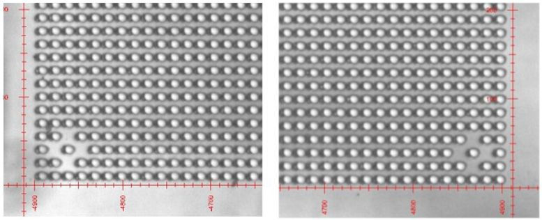
- Tool Levelling Station for co-planarity
Due to the height of the micro Indium bump array as well as the large component size, co-planarity is vital to the bonding process, to allow for even pressure and a parallel, even bond line across the entire bump array.
To compensate and correct the co-planarity of the tooling, a passive levelling method is used that can correct tool co-planarity to within < 0.5 μm over a 25 mm tool surface.
![Figure 6. [left] ~ 5 μm co-planarity error (more compression on the top left, no contact bottom right). [right] < 1 μm co-planarity error (even compression over the full 10 mm2 area)](https://static.wixstatic.com/media/090711_a58918db702847d1a08a417c643c516e~mv2.jpg/v1/fill/w_638,h_310,al_c,q_80,enc_avif,quality_auto/090711_a58918db702847d1a08a417c643c516e~mv2.jpg)
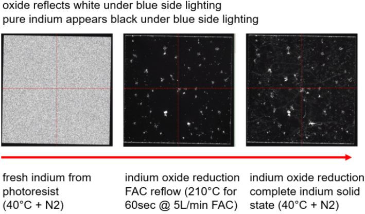
- Inert Gas / Formic Acid
For reflow and formic acid reflow bonding processes the bonding area was supplied with an inert gas to create an inert environment using Nitrogen (N2), or a processing gas such as Formic acid vapor to reduce oxides on metal surfaces to expose fresh Indium bonding surfaces.
To reduce oxide on the Indium bumps or to reform the pyramid shaped bumps into more uniform and less amorphous spheres the Indium can be reflowed in a formic acid environment with a laminar flow to carry away the oxides.

Once formic acid reflow is complete the components can be observed to contain far less oxide, with a majority of the surface being pure Indium or a very thin layer of oxide covering the Indium making for a higher strength and higher electrical quality bond surface.
- Laser Height Measurement
The automated FINEPLACER® system includes a Laser Height Sensor Module for measuring and evaluating flatness, co-planarity, and bond line thickness (BLT). Using point height measurements or detailed line scanning, it generates sub-micron resolution surface maps. This enables in-situ analysis of bonded assemblies without requiring additional equipment.


III. Results
Flatness and co-planarity
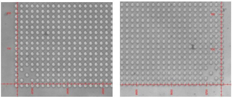
Optimizing the hardware and tooling design, in addition to the passive levelling of the tools enabled consistent, repeatable and controllable flatness and co-planarity in the bonds.
The flatness and co-planarity achieved on the 5 μm bump, 15 μm pitch 8x10 mm2 640x512 IR FPA trials was consistently below 1 μm.
![Figure 11. [left] ~ 5-6 μm co-planarity error. [right] ~ 1 μm co-planarity error](https://static.wixstatic.com/media/090711_29b2fe8899d14095be6247a02312f9f6~mv2.jpg/v1/fill/w_635,h_378,al_c,q_80,enc_avif,quality_auto/090711_29b2fe8899d14095be6247a02312f9f6~mv2.jpg)
(Newton ring effect, each 4 lines is estimated to be ~ 1 μm. Observed through transparent component, 130 N over 5 μm bump, 15 μm pitch 640x512 Indium bump array).
Accuracy
To develop the tooling requirements, bonding process and fine tune the bonding parameters a transparent chip with indium bump array was bonded to an ROIC with indium bump array. This trial was also used to assces post bond accuracy.
By optimizing the tooling, cleaning, process preparation and bonding parameters in combination with automated camera calibration processes, it was possible to consistently bond the components within 1 μm over many trials per day and maintain this quality over extended periods of time (1–2 weeks) without having to adjust the system.
Interconnect Quality
Real IR FPAs were bonded using these methods and underwent functional testing and stress testing for operation in cryogenic environments. Unfortunately these results cannot be shared but the results showed and interconnection yield of above 99% of the components with good dark current characteristics while withstanding high stress duty and temperature cycles.
IV. Discussion
Indium Bump Interconnect
Indium bump arrays are increasingly used in quantum computing, requiring precise co-planarity, bond line control, and high-quality interconnections. IR FPAs demand smaller, denser bumps, while consumer markets for micro-LEDs require higher throughput. These challenges will push die bonders to innovate further. Additionally, technologies like Cu-Cu wafer bonding for SWIR sensors will drive cost reductions and automation in Indium interconnect manufacturing.
V. Conclusion
Fine pitch micro Indium bump interconnect bonding is a challenging application, however using the methods described above it is possible to take this challenging bonding process and streamline it into a more stable low volume production process, removing risk of damage or failure while improving yield and bond quality in a more controllable and repeatable manner over sustained automated production cycles.
The FINEPLACER® femto 2 automated die bonder including the tooling and modules in combination with the improved cleaning and handling methods developed for this process, is an Ideal solution for low level production or research & development of any fine pitch micro Indium bump interconnect application for IR FPAs, quantum computing processors, X-Ray detectors or μLED displays for example.

VI. References
[1] IEEE 66th Electronic Components and Technology Conference, (2016): "A Room Temperature Flip-Chip Technology for High Pixel Count Microdisplays and Imaging Arrays "
[2] M Micro- and Nanotechnology Sensors, Systems, and Applications X, DOI:10.1117/12.2303735 (2018):
"Indium bump deposition for flip-chip micro-array image sensing and display applications"
[3] SONY "Short-Wavelength InfraRed Image Sensor Technology SenSWIR™"
[4] Department of Physics, ETH Zürich, CH-8093 Zürich, Switzerland (2023): "Improved Parameter Targeting in 3D-Integrated Superconducting Circuits through a Polymer Spacer Process”
MicroLED Manufacturing with Finetech – Accurate, Efficient and Scalable. Learn more about our die bonder solutions for MicroLED assembly and download our free technical paper at: https://go.finetech.de/l/1014812/2025-01-21/47pt2
Comments