Additive manufacturing of ceramics electronics is an interesting topic with applications in high-frequency and/or high-temperature electronics. This involves extensive process as well as novel material/paste development. CTTC is a center of competency in Limoge, France [one of the homes of ceramic technology in Europe], actively advancing this technology.
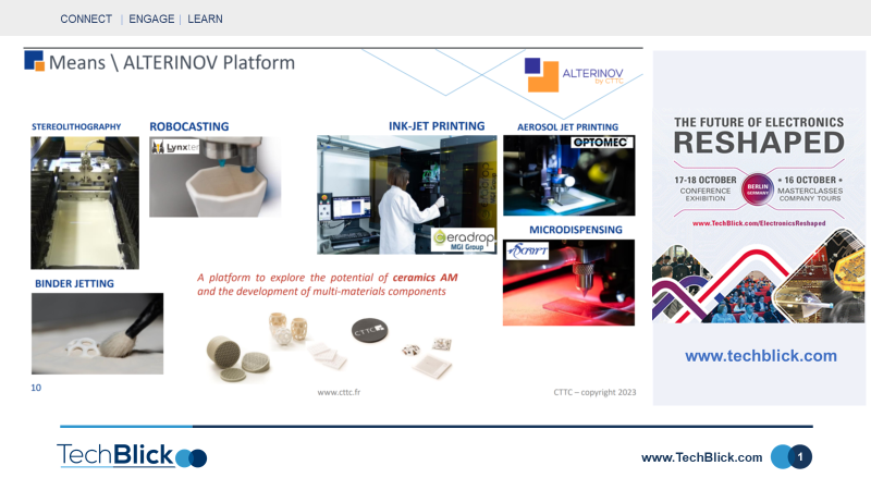
In their lab [slide 1], they have the following machines to develop fully 3D printed ceramic electronic devices
For 3D part: SLA, binder jetting, fused filament fabrication
For metallization: Inkjet printing [Ceradrop], microdispensing [nScrypt], aerosol jet printing [optomec]
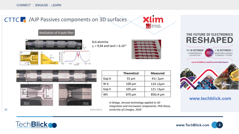
In slide [2] you can see a fully 3D printed 4-pole filter operating in the 40GHz range, developed in collaboration with xlim laboratories.
The structure was fully 3D printed using SLA [stereolithography] printed alumina, showing r = 9,94 and tan = 6.10^-4. The sides of the devices were metallized and using aerosol jet printing [AJP] an antenna structure was printed on the top with linewidths in the 100-120um range.
The table shows the dimensions of the theoretical and AJP printed structures, revealing around 15-20% deviation. Nonetheless, as the measured graph shows, the device exhibits good filtering properties at 40GHz. Note that SLA often yields a solid and smooth surface, which is important for subsequent metallization.
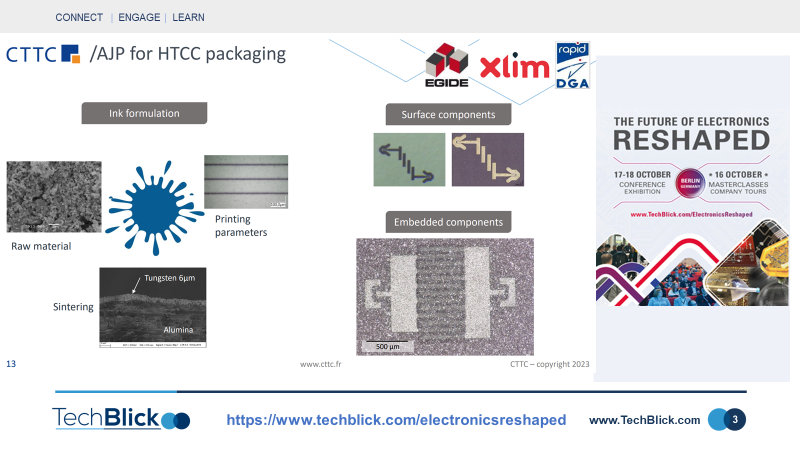
Slide [3] shows demonstrators for HTCC packaging which involves co-sintering at temperatures above 1000 C. Here, normal silver or copper pastes wont work, and new AJ printable pastes based on tungsten or Mo are needed. At CTTC, an AJ printable tungsten paste compatible with the HTCC process was developed, meaning that it could survive the high temperature sintering [>1000deg C]. This is an important achievement to develop novel high-T inks meeting requirements of HTCC sintering [both metal as well as alumina substrate] as well as AJ printing. As you can see, AJ printing could achieve 30um lines with 6um thickness on the underlying ceramic.
The two examples on the right show the realization of surface components as well as embedded components using AJ printing of these materials in HTCC packaging. For the surface components, the different between the two images is that the right image is sintered and gold plated [this explain the color change]
AJP is a good process with high resolution but only prints thin lines, and is thus not suited to application handling high currents. For such applications, microdispensing is a better application.
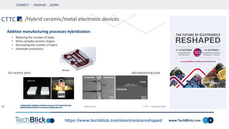
In slide [4] SLA was used to print the ceramic parts [alumina] while microdispensing was used to add the in-between conductive layers. Here too a novel paste needed to be developed. In this case, tungsten particles with 1.1um diameter and quasi-spherical grains were used. The paste had 39 vol% with cellulosic binder in aqueous media. It was designed to be dispensed through a 100 um diameter.
As seen also in slide [4] complex multi-layer HTCC structure with embedded metallized tracks/circuits were manufactured using this hybrid [SLA+ dispensing with complex high T sintering]. High frequency microstrip responses were also reported.[for on this see the work of J. Raynaud et al]
In the future hybridization of the dispensing with fused deposition process will be of importance. It will enable the 3D printing of larger HTCC parts, beyond what SLA allows.
Overall, this is an exciting development because it will allow full 3D printing of complex high-T ceramic [HTCC and LTCC] circuits with ever more complex shapes and thus ever more geometry-optimized properties. The automation of such process can also enable mass manufacture and mass customization of such complex geometries, going beyond what was previously considered the limit.
Join us and the global industry in Berlin on 17-18 OCT 2023 and LETS RESHAPE Electronics Together, making it Additive, 3D, Hybrid, and Sustainable https://www.techblick.com/electronicsreshaped


Yorumlar