Here you can see data - shared at TechBlick in March 2022- that shows rapid sintred Cu nanoparticles are a viable solution that meet most industry requirements.
First some background: the PV industry has tremendously progressed with a steep learning curve of 25%, meaning the cost drops 25% everytime the accumulated production capacity doubles.
The PV industry itself is now very large (around 183 Gwp in 2021 of new and replacement installation) but how large will it get in a net zero emission scenario in 2050? There will need to be an installed capacity of 20-80 TWp, producing 30-100 PWh of electricity. This will translate into an annual volume of 1-4 TWp/year, showing that there is still much room for expansion and thus innovation
Ag is a major cost driver of the PV cell today. Around 15mg/Wp is used in a PERC architecture for bus and finger metallization. Interestingly, not just cost but also availability can be a concern since 50% of today's world mining capacity would only cater for 1 TWp/a.
Given these concerns, the industry has long sought to replace Ag with alternatives such as Cu. However, many issues havehindered adoption even in new PV architectures including Cu diffusion into Si, solderability, good adhesion, long term stability, etc etc
In this study, Jan Lossen from ISC Konstanz shows that one can meet almost all requirements on a back-contact Si PV when the bus bars are screen printed using Cu nanoparticle pastes from Copprint. It also shows the good outlook for the case when also the fingers are replaced.
Slode show shows the difference between PERC and back-contact architecture. In the former, finger and bus bars (BB) on the front side are based on screen printed Ag, whilst Al metallization is used for the rear side. In the latter, the contacts for both polarities are placed on the rear side, thus leaving the front unshaded. If Ag were used this would mean even higher Ag content as both electrodes are Ag based!
In this study, the BBs were printed with low-T Ag pastes and various types of Cu pastes dried at 100C and sintered at 300C for 5s. You can see how the line resistance requirements are met by all Cu BB configurations. These BBs have 1.5mm width and 12um height. Furthermore, we see that the Jsc and Voc are not impacted.
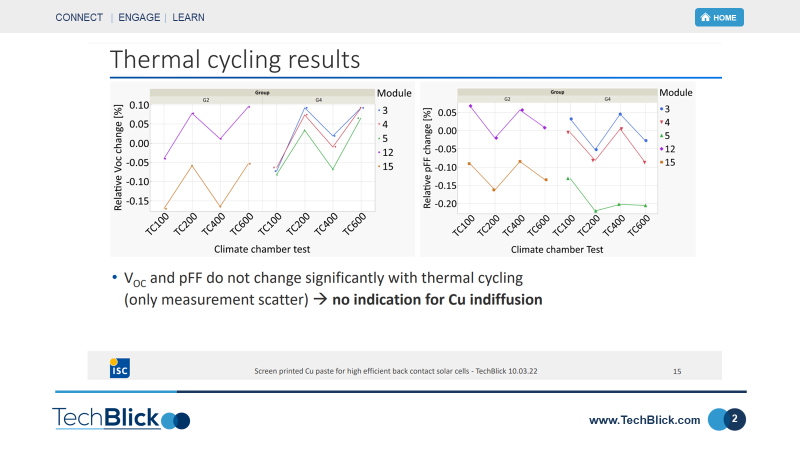
Climate chamber tests were also carried out, showing NO indication of Cu diffusion in thermal cycle and damp heat tests.
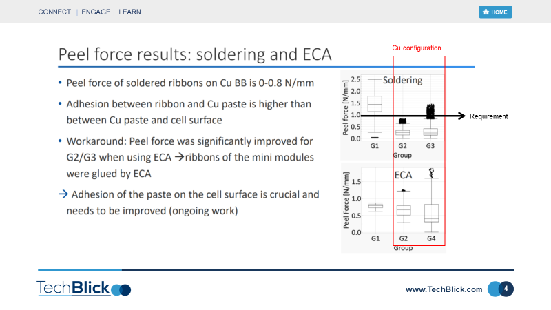
The remaining challenge here is the peel force. The slide below shows that one can can solder onto the Cu BBs the peel force is not sufficient, probably because of low adhesion between Cu and cell surface, requiring an ECA.
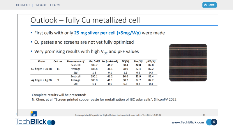
Final slide shows that fingers based Cu pastes also yield good results, suggesting that all Cu-based back-contact Si PVs are possible!
Ofer Shochet Dominik Rudolph Andreas Halm Yitzchak (Isaac) Rosen #solarcell #solarpanels #printedelectronics #copper #renewables


Comments