Conformal EMI shielding is a megatrend on its way to become ubiquitous in electronics. The incumbent process is based on sputtering a tri-layer structure consisting of SUS (stainless steel)- Cu-SUS (total stack is 3-6um typically) on the EMC (epoxy molding compound) of the package. Hikaru Uno from Merck & Melbs LeMieux from Electroninks Incorporated show an alternative based on non-vacuum spray coating of particle-free Ag inks. In these slides, you can see performance analysis and detailed cost analysis/projections.
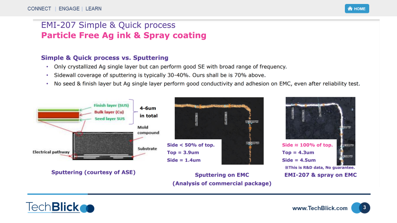
The incumbent (sputtering) is a well established technique with many market reference from the likes of Apple and Samsung. However, it is a vacuum process requiring substantial CapEx investments with a large production footprint. The sputtering deposition rate will also be low given the required film quality. Sputtering is poor at side wall and deep trench coverage, resulting in large thickness variations between the top and side walls.
Spraying the EMI shielding can address some issues: it is a non vacuum process with a low Capex and a high unit-per-hour (UPH) throughput and is able to offer uniform side and top wall coverage. The spraying can be used with Ag or Cu nanoparticles.
Both nanoparticle techniques though suffer from expensive materials, potential for nozzle clogging and thus production downtime, and even relatively thick required coatings.
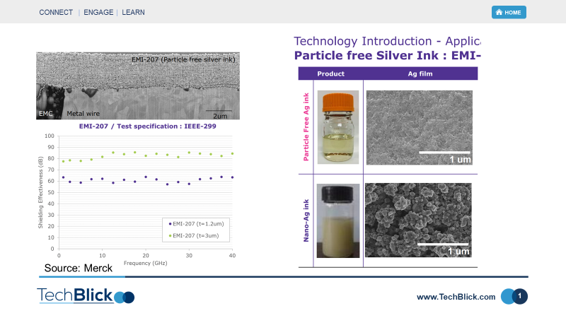
To overcome these shortcomings, particle-free silver inks can be sprayed.
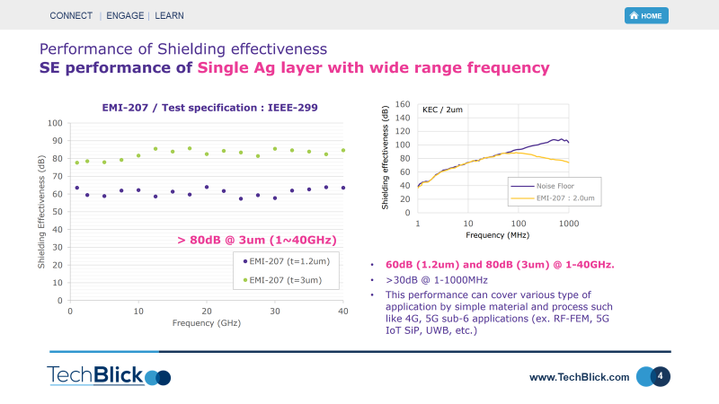
Is this technique effective? The below slides show shielding effective upto 40GHz with 1.2 and 3um coatings. This seems to meet the requirements.
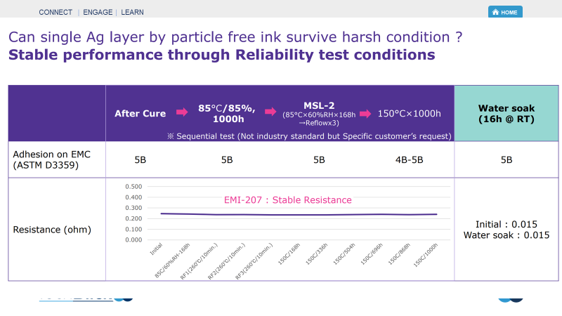
Is it reliable? In the slides below you can reliability data showing no measured change in sheet resistance of the package-level coated when subjected to a prolonged duration of harsh conditions
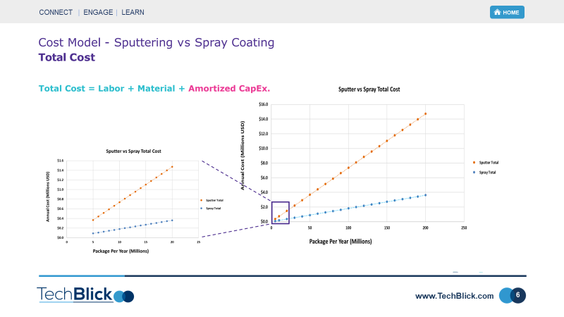
Is it cost effective? Sputtering has a high capex cost as well as relatively high labour costs. However, spraying has higher ongoing material consumption costs.The slides below shows that spraying can be a very cost competitive approach
Already commercial? It is still in sampling. The main stumbling back is the ever underestimate power of incumbency and already sunk CapEx investments in sputtering lines
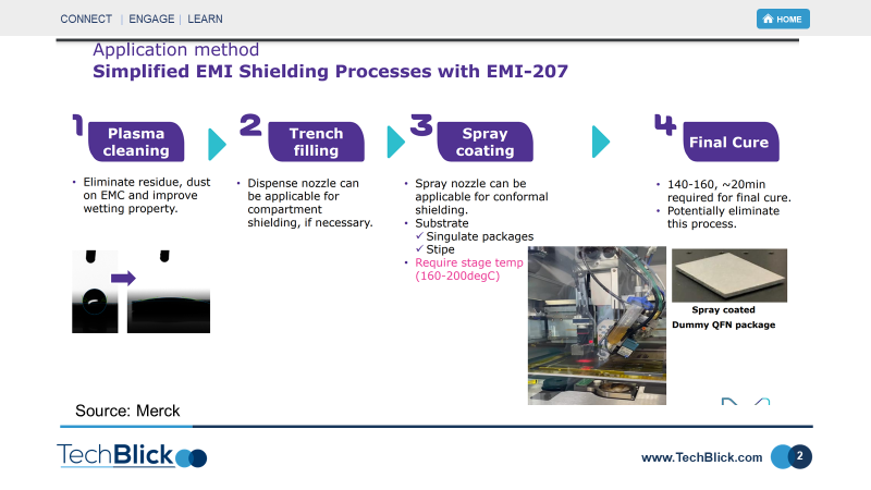
On the process, as shown below, the package is first pre-treated with plasma. The particle-free ink is then sprayed whilst the packages on the chuck are held at 160-200C. The elevated temperature results in rapid particle formation during the spray. Finally, after spraying, the inks are then cured for 20min@140-160C. There are relatively low curing temperature compared with other particle-free inks on the market.
With the first successful market reference using spraying, the market gates will open, lifting all ink-based techniques and making this a part of fast-growing electronic packaging industry
To learn more visit www.TechBlick.com TechBlick











Comments