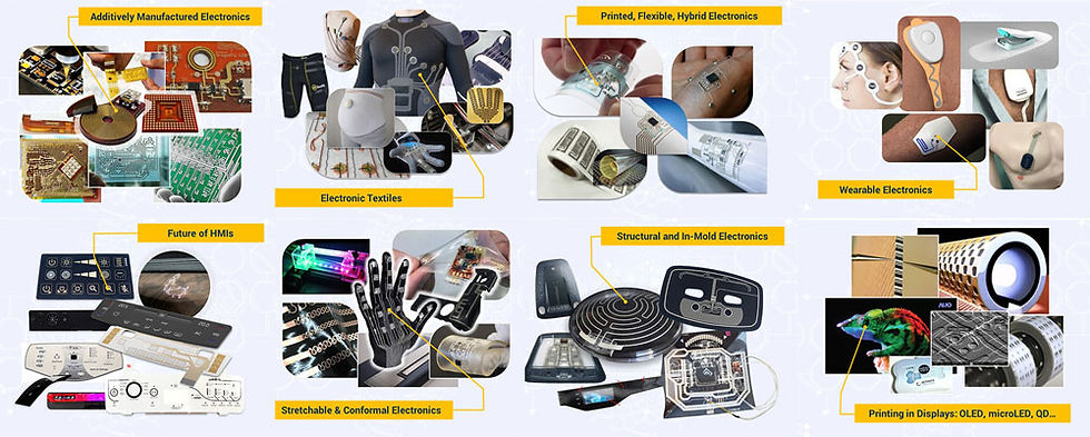
This newsletter will provide regular updates in additive electronics covering the full and broad spectrum of materials, processes, and applicaitons. The term additive electronics encompasses an exteremely diverse set of technologies and applications. We will cover all. To learn more visit TechBlick online or onsite (www.TechBlick.com).
Wrap-around electrodes for microLEDs
To scale up microLED displays to large areas, smaller displays can be titled. Because microLEDs can be truely edge-less devices, the tiling can function, yielding a seemless look.
Each title should house the microLEDs, backplane, as well as driver electrodes. The microLEDs and the backplane sit on the front side of the glass substrate whilst the driver electrodes are tucked away at the back. Interconnects are needed to connect the two. Wrap-around electrodes (interconnects wraping around the edge to connect front and back) is an elegent solution which bypasses the need for a drilled and filled through-glass via.
The wrap around electrodes can be printed or PVD deposited (both prefer chamfered glass) . The latter can yield better feature sizes and thin and conductive lines, whilst the former can increase productivity.
The below images demonstrate various technologies. Screen printing is a robust solution with low TACT time. Applied Materials has demonstrated that it can screen print very narrow (30um) linewidths over narrow spacings (50um). These are excellent results. Note, by way of reference, that state-of-the-practice/production and state-of-the-art in screen printing of conductive paste on silicon solar PVs are 35um and 20um, respectively. In the process, first the top and botton electrodes are printed before the substrate is rotated (with excellent alignment) to print the electrodes over the edge.

This technologies requires excellent machines. Applied Materials has launched a machine able to handle 230x230mm substrate with +/- 6um repeatability and a throughput of 1000pph. Note that optimization of the past and print process are critical. In general, a paste with very high conductivity (20% bulk Ag) with 5B adhesion onto glass will be needed. The target final printed thickness is 3-5um. The screen printing process should yield smooth surface with no peaks near the edge.
Aerosol jet is also being proposed for additive deposition of wrap-around electrodes. The advantage of aerosol is that it can print over 3D surfaces and that it can in general deposit fine features than screen printing. To achieve wrap-around electrodes, two half-wrap electrodes must be printed (see below). In between the steps, the glass will need to be rotated. Optomec claims to achieve 18k full-wrap interconencts per hour (excluding the time it takes to rotate the glass). Note that the example below shows L/S 50um although, in principle, aerosol jet can go from down.
In general, this is an interesting solution for the microLED market
Impulse Printing- the master of all printed electronics process?
Impulse Printing- unveiled and presented recently at TechBlick- seems to be an exciting technology. The technology details are not yet fully disclosed, and the development is still at a laboratory stage, but the disclosed results and claimed performance levels are incredible.
As you can see below, the technology can digitally print tracks with resolutions as low as 2um and as high as one millimeter. It can print materials with an extremely wide viscousity range, from 0.1 to 10,000 Pa.s, meaning that it can print copper and silver inks as well as solder and epoxy(!) based conductive adhesives! The technique prints over 3D surfaces, able to print over gaps as short as 1um and as tall as 10mm. This digital printing technique can print sequential as well as simultaneous patterns at high speeds.
The diversity in all paramters (resolution, print gap, viscosity of ink or pastes, etc) is very unique for any digital pritning process. Indeed, as shown in the chart belows, each technology occupies a given position in terms of resolution/feature size, viscosity, print gap, etc).
The technology is still young and in development. Today, the print area is small (1x10mm2) but there is a roadmap to scale the tool to be able to print first at 20x20mm2 and then 96x96mm2.
Watch this space as the technology will soon be spun out into a start-up!
Taking the accuracy of printed electronics below 1um
Printed electronics technology is evolving. A development direction is ultrafine line printing, increasingly allowing the technology to encroach into the realm of photolithography. The example here, developed by VTT, demonstrate a process for sub-micron printing.
The process is reverse offset printing. Here, the PDMS roller is first coated with the ink. The ink semi-dries on the roller, partially through absorption into the PDMS. This semi-dried state allows one to overcome wetting-related issues when inks are in liquid state. The inked PDMS roller is brought into contact with a Cliche, or relief plate, removing parts of the inks. The patterned semi-dried inks on the PDMS roller are then transferred onto the final substrate.
In this example VTT achieves 1µm direct printing of silver nanoparticle inks. The desktop RO printer was used to print a metal mesh on PET with 1µm linewidths. The reported sheet resisitivty is not very low (100Ohm/sqr), probably because the lines are very thin.
In general, note that ROP can enable minimum resolutions between 0.5-5µm, printed thickness lines around 20-1000nm, overlay accuracy <2um, and printing speeds of 50mm/s (3m/min).

Advanced Interconnect Solutions for Flexible Hybrid Solutions
Flexible Hybrid Electronics (FHE) brings together the best of printed and flexible electronics with rigid Si-based electronics. A critical and often limiting bottleneck is the interconnect between printed (often wide) and Si ICs (often narrow pitches). Normal solder can not easily be used because (1) substrate such as TPU (stretchable electronics) and PET (flexible electrodes) impose severe temperature limitation, often even below bismuth-based low-T solders, and (2) some inks, specially Ag inks, dissolve in solder. Furthermore, these interconnects need not only support the pitch sizes of the ICs, but also survive flexibling as well as stretching, and be compatible with standard industry processes.
One option is to deploy particle filled (often Ag particle) epoxies to form the interconnects. Here, unless it is anisotrophic, then the pitch sizes will be limited. Furthermore, particle loadings are often high to achieve high conductivity, adding to cost.
Sunray Scientific Inc has developed a novel solution: they disperse ferromagnetic particles within a two-part epoxy system. Under an external magnetic field, the particle align vertically, forming z-axis conductive paths. Here, the pitch can be down to 100um. The curing temperature can be as low as 80C, making compatible with TPU and PET. The material can sustain extreme repeated stretching.
Furthermore, the process is, as shown below, compatible with standard SMT process. The material can be stencil printed or dispensed. Once the component is pick and placed, a magnetic pallet is used to align the particles before sending the film through a curing step (batch over, reflow, vertical oven)
This is an interesting process. It of course lacks the self alignment properties of solder. The ptich is also currenly limited to 100um, which is too wide for many ICs.

Solderable highly conductive Cu nanoparticle inks?
A major challenge in printed electronics is the inability to solder directly on Ag paste (the most common ink and paste material) because no intermetallic layer is formed. With Cu, this can be different.
Here, Copprint is showing results, demonstrating that one can directly solder onto their Cu pastes with good shear test results, even if sometimes the wetting is not the best. It also shows how a strong intermetallic layer is formed during the solder, for example, with the standard SAC305 solder on an FR4 substrate.
This is an important advancement of the art because it makes printed electronics more compatible with standard SMT processes. Furthermore, the Cu ink is compatible with low-T solders too, enabling one to solder components directly onto a PET substrate with printed Cu lines.
In general, Cu inks have had issues in the past. The conductivity has not been high enough, meaning more material is needed thereby eroding their $/Kg advantage vs. Ag. They have also required novel sintering steps with a new learning curve and with new equipment. The data from Copprint suggests that their ink can be sintered very fast and achieve conductivity levels outperforming those of classic Ag suppliers.


Comentários