


10 April 2025
Sustainable Inks, PTC Film Heater Design, Next, Gen Battery Separators, ePaper Advances, Novel Silicone Technology
In this edition, we look into materials science, energy storage, printed electronics, and sustainable display technologies. Joanneum Research introduces Supresil®, a patented technology that optimizes the processing window for platinum-cured silicones (LSR and HCR) without compromising material properties, ideal for 3D printing. Celanese Micromax presents PTC film heaters, leveraging Joule heating and printed carbon pastes for uniform, self-regulating thermal solutions across flexible substrates. AilArian addresses the environmental impact of metal-based conductive inks in biodegradable electronics with a novel magnetic separation technique for recovering silver, promoting both high conductivity and eco-friendliness. Sepion Technologies reveals a new battery separator coating that improves moisture resistance, enhances safety, and reduces manufacturing costs, enabling the use of low-cost cathodes. Finally, E Ink compares ePaper with emissive displays, focusing on energy efficiency, readability, and use cases in retail, public information, and digital signage. Joanneum Research | New inhibition technology for (Pt)-cured silicones (LSR and HCR) to optimise the processing window without changing material properties - Supresil® Celanese Micromax | PTC Film Heaters – Materials, Design and Applications AilArian | Magnetic separation of silver conductive material for fully biodegradable electronics Sepion Technologies | The Next-Generation of Battery Separators Eink | ePaper ...

9 April 2025
Innovations Tour in Additive Electronics: From Analog to Digital Printing | Fineline, high viscosity, and 3D
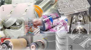
In this article, we highlight a number of printing process innovations that are advancing the state of the art in printed and additive electronics and are addressing critical existing limitations to open new opportunities. Here, we will go on a quick tour from analog screen printing to digital printing to ink-less laser printing. In this journey, we will make many short stops covering screen printing, capillary printing, inkjet printing, EHD printing, micro-dispensing, LIFT printing, dry printing and beyond. Wit over 25 images, tables, charts as well as 13 videos, we cover the following points Screen printing: State of the art ultrafine line printing High production speed in screen printed metallisation Rotary screen printing for PV metallisation Alternative PV metallisation methods (1): Capillary printing Digital printed electronics/additive electronics Can we scale up inkjet printing in functional printing? How to digitally print high viscosity pastes? Digital multi-material laser printing of high viscosity pastes in printed electronics and electronics manufacturing High viscosity digital printing AND ultra fine resolution well beyond inkjet or LIFT Digitally printing higher viscosity levels at ultrafine resolution without e-field? High Pressure Capillary Printing - high resolution, high aspect ratio and high viscosity printing without e-fields, satellites or splashing? Printed Electronics / Additive Electronics without inks? SSAIL Process: Additive laser-induced metallis...

3 April 2025
Material Innovations: QD color conversion, copper inks for printed electronics, indium solder bumps for microLEDs, battery Safety in Na batteries, and more
Fraunhofer IAP | Quantum Dot Color Conversion in MicroLED – A Material Perspective - Quantum Dot (QD) materials for color conversion in MicroLED displays. Key topics include high quantum efficiency QDs, tailored ink formulations, and EHD-Jet printing techniques for high-resolution applications. The session explores QD stability, ligand optimization, and methods to close the green and red gap in MicroLED displays. Saralon GmbH | Conducting Copper Ink for Printed Electronics: An Application-Based Journey - Saral Copper Ink as an alternative to costly silver-based inks for printed electronics. The session covers copper ink’s stable conductivity, processability via conventional screen printing, and its application in low-cost, high-demand sectors. It highlights challenges and benefits for future electronics manufacturing. INTLVAC THIN FILM | ICARUS: Indium Solder Bump Deposition System- Focusing on improving indium solder bump deposition, addressing pattern hole closure, dendritic growth prevention, and enhancing bump quality. Insights on system stability and reliability for semiconductor assembly and MEMS packaging will also be discussed. Flexoo | Excellence in European Manufacturing: Focus on Contract Manufacturing and R&D Services- Exploring mass-customization in high-end sensing solutions. Topics include the production of BaMoS and MiniMoS sensors, battery behavior analysis at the cell level, advanced wiring solutions, and the role of digitalized processes in manufacturing ef...

27 March 2025
Wearable Neurotechnology, Printed Dielectrics, OTFTs, Jetting Electronics, R2R OPV for Energy Harvesting
Wearable neurotechnology, printed electronics, OTFT displays, and light energy harvesting. Researchers at Stanford University are developing innovative neurosensing and neuromodulation technologies, including fNIRS headbands for monitoring mental states, ultrasound neuro-immunomodulation for treating Parkinson’s disease and stroke, and e-Skin EMG sensors for improved prosthetic control and gait correction. ChemCubed is advancing inkjet printing for multilayer electronics, using ElectroJet™ nanoparticle-free silver conductive ink and high-performance dielectric materials to create advanced circuit boards for capacitors, sensors, and antennas. SmartKem is scaling up its low-temperature OTFT technology for AMOLED and MicroLED displays, leveraging TruFlex™ organic materials that enable flexible, solution-based electronics with low-NRE processing and ULEF integration for ultra-low energy consumption. Epishine is eliminating the need for disposable batteries in connected sensors by harnessing ambient light energy, creating self-charging battery technology that extends device lifespan and reduces environmental impact. Essemtec is optimizing conductive adhesive dispensing for printed electronics manufacturing, improving reliability and efficiency through rheology optimization and jetting technology. Stanford University | Looking ahead – Research topics in wearable neurotechnology innovations from Stanford University ChemCubed | Printing Dielectric Layers in Multilayer/Multimaterial...

9 April 2025
Repairing Open Defects in Semiconductors: A Key to Sustainable Manufacturing
The Evolution of the Semiconductor Industry and Its Path to Sustainability Author: Elisa DUQUET, Hummink, elisa.duquet@hummink.com The semiconductor industry is one of the most complex, dynamic, and technologically advanced sectors in the world. It plays an essential role in shaping modern life, serving as the foundation for everything from smartphones and MRI machines to kitchen appliances and space shuttles. In today’s digital world, nearly every device we rely on is powered by semiconductor chips. The demand for semiconductor chips has reached unprecedented levels. According to the Semiconductor Industry Association (SIA), the industry shipped a record of 1.15 trillion semiconductor units last year, this figure means that every person on earth could receive over 150 chips annually. In addition, the SIA announced that the global semiconductor sales hit $627.6 billion in 2024, an increase of 19.1% compared to 2023. The semiconductor industry is projected to reach over $726.73 billion by 2027. We are Exhibiting! Visit our booth at the TechBlick event on 11-12 June 2025 in Boston . Contact us for your special discount coupon to attend (elisa.duquet@hummink.com) As production scales up to meet increasing demand, so does the need for sustainable solutions to manage waste and defective components. Indeed, the twelve largest semiconductor manufacturers together generate about 2.7 million tons of waste annually - about as much as 5 million EU citizens. Nearly 50 percent of the ...

8 April 2025
Saralon | New Ink Sets for Stretchable Printed Electronics Applications
Author: Steve Paschky Saralon now offers new ink sets for stretchable membrane switches, heaters, and electroluminescent display printing. Each of these sets contains all the essential ink components tailored to each application, simplifying your work for a seamless, high-quality experience. We are Exhibiting! Visit our booth at the TechBlick event on 11-12 June 2025 in Boston Last year, I wrote about our range of stretchable Saral Inks , designed for different substrates with various formulations like silver, carbon, and others. Since then, technology has continued to evolve, and so have the needs of the industry. We’ve been hearing from customers that they need stretchable inks that are not only conducting but also provide features like heating and capacitive touch, all while withstanding dynamic forces like bending, stretching, and twisting. One of our major focuses at Saralon has been on providing "ink sets"- collections of compatible inks that are designed for specific applications of Printed Electronics (PE). This approach aligns with our company’s mission: Simplifying Electronics Through InkTech. PE devices often require printing multiple layers of ink on top of each other, and one common challenge for developers is finding the right combination of inks that work well together. That’s where our Saral Inks Sets come in. For specific PE applications, we offer complete sets of inks that are compatible with one another, easy to print, and ensure a trouble-less printing pro...
31 March 2025
Additive Printed Electronics Advances: 3D Additive Lithography, R2R Pilot Line, Micro-Dispensing, Gravure Printed Micro-Bumps, Ultra Fineline Metallisation, Anisotropic Conductive Adhesives
In this newsletter you can learn about the latest advances in Additive, Sustainable, Hybrid and 3D Electronics! via the following highlighted short videos, each being less than 2min, saving you learning time. These are all key points and advances in the field, advancing the art and cutting-edge. R2R pilot hybrid electric manufacturing line for wearable sensors? | VTT What are the real applications of ACFs (anisotropic conductive films)? | CondAlign How is micro-dispensing positioned and how fast can it print? | XTPL How to print silver lines finer than human hair on Si photovoltaics | Fraunhofer ISE How does the 3D additive lithography for additive electronic work? | Holst Centre Why is there a need for direct gravure printing of manufacturing solder bumps? | Komori The Future of Electronics RESHAPED USA Conference and Exhibition #AdditiveElectronics #3DElectronics #PrintedElectronics #WearableElectronics #FlexibleHybridElectronics #WearableElectronics #SustainableElectronics #ElectronicTextiles 🗓️ 11 & 12 June 2025 📍 Boston, USA 🔗 Agenda & Registration: https://www.techblick.com/electronicsreshapedusa 🎤 70+ World-Class Speakers 🏢 75+ Global Exhibitors 👥 550+ Participants from Around the World 🛑🛑 In addition to the early bird rates, there is a special one-time promotion offering an additional 200 USD discount. Get your coupon here . The early bird rates expire on 25 April 2025. 🛑🛑 R2R pilot hybrid electric manufacturing line for wearable sen...

25 March 2025
Introducing the Program: Process Innovations | Molten metal jetting, R2R LIFT printing, microscale laser sintering for 3D interconnects, DLP for complex interposes, direct write ALD, stable AJP
TechBlick's The Future of Electronics RESHAPED USA - Why You Should Join Us? The Future of Electronics RESHAPED USA is less than three months away. It features a world-class agenda with over 70 presentations covering exciting material breakthroughs, process innovations, manufacturing advances, application developments, and product launches. See the program here. In this article series, we highlight various talks in the program, outlining the technologies and applications that will be showcased. In this particular article, we focus on process innovation, highlighting a diverse set of technologies, including multi-head molten metal jetting, R2R LIFT printing, microscale laser sintering for 3D metal interconnect, DLP for complex interposes, direct write spatial atomic layer deposition, and stable aerosol jetting. In subsequent articles, we will focus on wearable and printed electronics, 3D electronics, sustainable electronics, material breakthroughs, manufacturing advances, novel applications, process innovations, and more.
It is time to join the global Additive, Printed and 3D Electronics movement: The Future of Electronics RESHAPED USA
🗓️ 11 & 12 June 2025 📍 Boston, USA 🔗 Agenda & Registration 🎤 70+ World-Class Speakers 🏢 75+ Global Exhibitors 👥 550+ Participants from Around the World The early bird rates expire on 25 April 2025 .
In addition to the early bird rates, a special one-time promotion offers an
additional 200 USD discount.
Do NOT forget to bo...