


17 January 2025
R&D Funding Opportunities, Flexible Printed Electronics, Advanced Battery Technologies, and IoT Applications
TechBlick wishes you a wonderful 2025! In this edition, we highlight, NETO Innovation specializes in securing funding for R&D projects through programs like Horizon Europe, EIC, and Eureka, with expertise in green energy, printed electronics, healthcare, and advanced materials. Yamagata University showcases advancements in flexible, printed carbon-based sensors for IoT applications, focusing on high-sensitivity pressure, strain, and humidity sensors for robotics and healthcare. Ensurge leads in anode-less solid-state lithium microbattery technology, offering superior energy density, rapid charging, and ultrathin packaging to address scale-up challenges for IoT and wearable devices. Kimoto presents cutting-edge adhesive and protective film solutions for precision manufacturing, including residue-free adhesives, high-transparency coatings, ESD protection, and advanced converting techniques like die-cutting and laser cutting. As we enter 2025, we’re excited to continue sharing the latest insights, trends, and opportunities in emerging technologies. Thank you for your continued support we look forward to connecting with you in our upcoming events. NETO Innovation | Unlock your project's full potential with NETO Innovation Yamagata University | Flexible Printed Carbon-based Sensors and Their Applications Ensurge | Manufacturing Scale-Up of mAh Class Anode-less Solid-State Lithium Microbatteries Kimoto | Adhesive Carrier and Protection Films for Advanced Manufacturing Join us o...

8 January 2025
Time to Book Your Place for 2025
TechBlick's Future of Electronics RESHAPED conference and exhibitions in 2024 were enormous successes with record participation. Thank you very much to all those who participated. And even though we are only at the start of 2025, our capacity is filling up fast at both our events. The Only Global Event On Additive Electronics, Printed Electronics, Hybrid Electronics, and Sustainable Electronics TechBlick is the only global offering in the field, combining onsite events in the USA and in Europe with an incredible online event series to reach the entire industry around the world. We had an incredible 2024 and are super excited about 2025. In Boston 2024 we had a sell-out event in the USA (Boston) bringing together the entire printed electronics industry. This event is now the largest and most important event in the field in North America. And we expect over 50% growth in 2025 vs. 2024. In Berlin 2024 we also had a fantastic and sell-out event. This remains our flagship event with a fully booked exhibition floor and over 550 participants. Our two online Innovation Festivals also continued to attract record participation with over 1600 registrants from right around the world Book Your Place NOW We strongly recommend that you book your place soon for 2025. Spots will be assigned on a first come first served basis. For Boston 2025, more booths than the entire 2024 exhibition are already booked. In fact, almost 80% of the expanded capacity is sold out. For Berlin 2025, nearly 65%...

6 January 2025
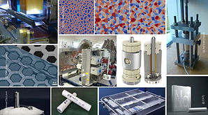
ATLANT 3D: Transforming Advanced Manufacturing with Direct Atomic Layer Processing (DALP®)
In today’s world, semiconductor microdevices form the backbone of nearly every piece of modern technology. Manufacturing these tiny devices is a complex, multi-step process involving both additive (vapor deposition, sputtering) and subtractive (dry or wet etching) techniques. The key to success in this process is photolithography — a method that uses UV light to define patterns through specialized masks. But photolithography requires cleanrooms — highly controlled, particle-free environments. These facilities, marvels of engineering, are necessary to ensure contaminants don’t compromise device designs, but they come with significant costs and energy demands. Cleanrooms must operate with extreme precision, filtering the air to the highest standards and maintaining constant supplies of distilled water, pressurized gases like argon and nitrogen, and facilities to handle chemical waste. This intricate setup, while effective, is not only expensive but also energy-intensive, making it a significant bottleneck in manufacturing efficiency. The Promise (and Limitations) of Additive Manufacturing In recent years, additive manufacturing — more commonly known as 3D printing — has been heralded as a potential game-changer for many industries. From printing microscopic plastic parts to entire boats and even human tissue, additive manufacturing offers flexibility that traditional fabrication methods lack. However, for micro- and nanofabrication , 3D printing technologies like laser-based...

19 December 2024
World's First System for Testing AR Contact Lenses
Authors: [1] Dr. Kedar Sathaye , Product Manager Light & Display at Konica Minolta Sensing Europe B.V. [2] Dr. Valentyn Volkov , co-founder of XPANCEO The market for image display devices is rapidly evolving, with innovations ranging from advanced screen technologies in smartphones and TVs to more sophisticated solutions like augmented reality (AR) glasses and virtual reality (VR) headsets, such as the Apple Vision Pro. The XR market alone is projected to reach an impressive $1,913.7 billion by 2032, with a growth rate of 39.2% from 2024 to 2032. There’s an increasing focus on making these devices more wearable and user-friendly. Achieving this goal, however, presents significant challenges due to the limitations of current technologies. Wearable devices, particularly in the AR and VR sectors, often face critical performance issues. For example, AR glasses and VR headsets frequently lack sufficient brightness, have limited battery life, and often end up being bulky due to the need for larger batteries. These issues can lead to overheating and reduced field of view, decreasing the practicality of these devices for long-term use. This is driving the industry to innovate and develop new devices that overcome these challenges. However, this rapid development invites another problem: the lack of comprehensive test solutions to ensure that these new devices meet the required standards for quality, safety, and performance. In response to this gap, Konica Minolta and XPANCEO have p...

15 January 2025
Voltera: Printing a Flexible PCB with Silver Ink on PET
LED applications are popular engineering projects in school. Among these, an LED roulette stands out as it is intellectually challenging and fun. While a roulette circuit is typically printed on a substrate like FR4, printing on a flexible substrate presents further opportunities for education. Contact: sales@voltera.io or +1 888-381-3332 ext: 1 Summary of Materials and Tools MATERIALS USED Voltera Conductor 3 silver ink ACI Materials FS0142 Semi-Sintering Conductive Ink ACI Materials SI3104 Stretchable Printed Insulator Voltera T4 solder paste Voltera solder wire Siraya Tech Tenacious Flexible Resin SUBSTRATES USED Normandy Coating polyethylene terephthalate (PET) FR1 board TOOLS AND ACCESSORIES V-One PCB printer NOVA materials dispensing system Voltera disposable nozzle Nordson EFD 7018395 dispensing tip Nordson EFD 7018424 dispensing tip Nordson general purpose dispense tips NE555DR timer LEDs Project Overview Purpose The goal of this project was to prototype a flexible multilayer LED wheel roulette circuit that was traditionally considered rigid and validate the redesign of the circuit. Design This project involves a multilayer flexible PCB for the LED roulette circuit and a traditional control board that powers it. We adapted the design of an LED roulette circuit, originally developed for a 3” × 4” FR4 board by ITIZ , Voltera’s authorized reseller in Korea. This new version is printed on a coated biaxially oriented PET substrate, allowing the circuit to remain...

6 January 2025
Break-through for novel red-emitting pyramidal microLEDs, based on the same InGaN material system as the green- and blue-emitting
Author: Oskar Fajerson , CEO, Polar Light Technologies With Polar Light Technologies’ novel concept, based on a non-etching bottom-up approach, red light at 625 nm has been achieved. By this remarkable breakthrough, Polar Light Technologies have reached red, green and blue pyramidal microLEDs employing the same material system. Polar Light Technologies has attained this milestone after more than 15 years research work and development. These novel microLEDs will open the gate towards future spatial computing and next-generation panel displays. The concept with the pyramidal design employed by Polar Light Technologies, will allow the ability with manufacturable microLEDs, while still maintaining their outstanding performance. Accordingly, the pyramidal microLEDs are ideal candidates for monolithic RGB displays. Red LED emission without compromises Due to the nitride material properties, there is an increasing challenge to realize efficient microLEDs as one goes towards longer wavelengths. While blue and green microLEDs have been on the market for years, reaching the red color is facing fundamental challenges due to the internal lattice-mismatch. Red color microLEDs have been demonstrated and reported, but they come with different compromises, such as manufacturability or the need to combine with other material systems. “Pursuing Polar Lights’ innovative pyramidal LED concept has been about overcoming those challenges without compromises. Today, thanks to a great tech team, we h...
23 December 2024
Carbon Nanomembranes for Metal Anodes, Solid-State Battery Materials Testing, Sodium-Ion Batteries, and Roll-to-Roll Manufacturing Innovations
This issue of the TechBlick newsletter highlights battery technology, featuring insights from industry experts. Albert Schnieders from CNM Technologies discusses how Carbon Nanomembranes (CNMs) are enabling metal anode batteries by preventing dendrite growth and improving performance with standard separators. Dr. Christoffer Karlsson from rhd Instruments covers the improvements in solid-state battery materials testing through active pressure and temperature control. Rene Windiks from Materials Design explores atomic-scale modeling to optimize battery materials and enhance performance and safety. Marja Vilkman from VTT introduces the SOLiD EU project, focused on sustainable manufacturing and Roll-to-Roll (R2R) processes for solid-state batteries. Lastly, Shmuel De-Leon examines the growing sodium-ion battery market, its advantages and limitations, and the future of mass production. CNM Technologies | Enabling metal anode batteries by modifying the anode & separator interfaces with Carbon Nanomembranes rhd Instruments | Improving Solid State Battery Materials Testing through Active Pressure and Temperature Control Materials Design | Advancing Battery Materials Through Atomic Scale Modeling VTT | The development of R2R processes for manufacturing solid state batteries. The newly launched SOLID EU project Shmuel De-Leon | Sodium Ion (Na- Ion) Battery Market 2024. The Next Technology on Battery Mass Production Register by end of December and save 150 Euros! Use discount cod...
19 December 2024
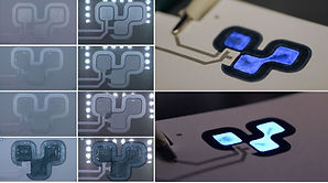
Voltera: Printing Electroluminescent Ink on Paper and PET
As presented at the recent TechBlick’s Future of Electronics RESHAPED USA event held in Boston, our project, Multilayer Flexible Displays Using Electroluminescent Ink , validated the use of the Voltera NOVA material dispensing system to print a multilayer electroluminescent display on PET and paper using various Saralon inks. In this article, we explain how this project was achieved, covering the inks and substrates used, the steps we followed, as well as challenges and tips on printing flexible multilayer projects using the direct-ink-write technology. Contact: sales@voltera.io or +1 888-381-3332 ext: 1 Summary of Materials and Tools MATERIALS USED Saralon Saral Silver 700 Silver-Based Conductive Ink Saralon Saral Dielectric 600 Dielectric Ink Saralon Saral BluePhosphorl 800 Electroluminescent Ink Saralon Saral Conducting Polymer 700 Polymer Electrochromic Ink SUBSTRATES USED Polyethylene terephthalate (PET) Cardstock paper TOOLS AND ACCESSORIES Nordson EFD 7018424 dispensing tip Nordson EFD 7018333 dispensing tip Nordson EFD 7018482 chamfered tip Adafruit 12V EL wire/tape inverter Project Overview Purpose The purpose of this project was to demonstrate the multilayer capability of Voltera NOVA . We printed a blue light-emitting pattern - the Voltera logo - on two substrates: paper and PET separately, using electroluminescent ink. Design layout Electroluminescence operates by exciting a phosphor material with an electric field. An inverter is needed to convert the direct...